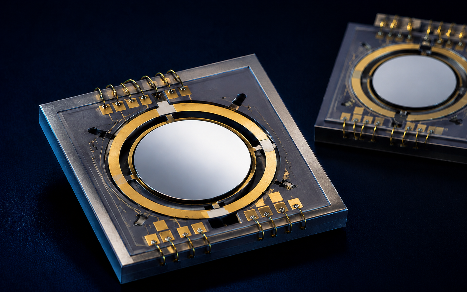
Swiss foundry partner for AI-designed multi-material semiconductors: piezoelectric MEMS, photonics and compound semiconductors through to wafer-level volume production

25FAB GmbH
CH-5234 Villigen (Switzerland) · Head office and business addressNew on Amplifa
About 25FAB
25FAB GmbH is a Swiss company for advanced manufacturing and volume production of AI-designed, multi-material semiconductor technologies. The company combines AI-supported device optimization, wafer-level multi-material integration and metrological validation, and supports programs from specification through engineering wafers and pilot lots to recurring volume production of chips and modules. Manufacturing is performed at wafer level across piezoelectric, photonic, III–V, wide-bandgap and heterogeneous material systems, including PMUT arrays, piezoelectric MEMS microphones, loudspeakers and micromirrors, piezo-tunable photonic integrated circuits, and metasurfaces. For custom components, MPW and dedicated wafer runs are available; selected programs achieve first engineering validation in around three months, with a scaling path to 8-inch production. The company is headquartered in Villigen in the canton of Aargau; manufacturing is performed worldwide for OEM and deep-tech customers from the semiconductor, MEMS, photonics, quantum and sensor sectors. Customer files, designs and intellectual property are treated under strict confidentiality.
- Site
- CH-5234 Villigen
- Processes
- PMUT manufacturing (piezoelectric ultrasound arrays, large arrays 32 to 1,024+ elements), Piezoelectric MEMS loudspeakers (wafer-level), Piezoelectric MEMS microphones, Piezoelectric MEMS micromirrors (1D/2D scanning, beam steering), Piezo-tunable PIC (integrated photonics with piezoelectric actuation, ~1550 nm), PIC manufacturing (photonic integrated circuits, wafer level), Metasurface/metalens manufacturing (flat optics), SiC platform (semiconductor and MEMS processes for high power/harsh environments)
- Materials
- PZT (lead zirconate titanate), AlN (aluminum nitride), AlScN (aluminum scandium nitride, ≤40% Sc), BTO-on-Si (barium titanate on silicon), Silicon nitride, SOI (silicon-on-insulator), Ge-on-Si (germanium on silicon), GeSn (germanium tin)
- Industries
- Semiconductors/semiconductor manufacturing, MEMS, Photonics/integrated photonics, Quantum Photonics/quantum systems, OEM electronics, Deep tech
- 01
Design briefing and feasibility check
- 02
AI-supported device design (FEM/electromagnetic simulation, layout/GDS)
- 03
Custom development and process integration
- 04
Engineering samples / prototypes and engineering wafers
- 05
MPW / dedicated runs
- 06
Packaging and module integration
- 07
Wafer-level volume production with quality control
Locations
Villigen
CHBusiness address / head office
Components & Modules
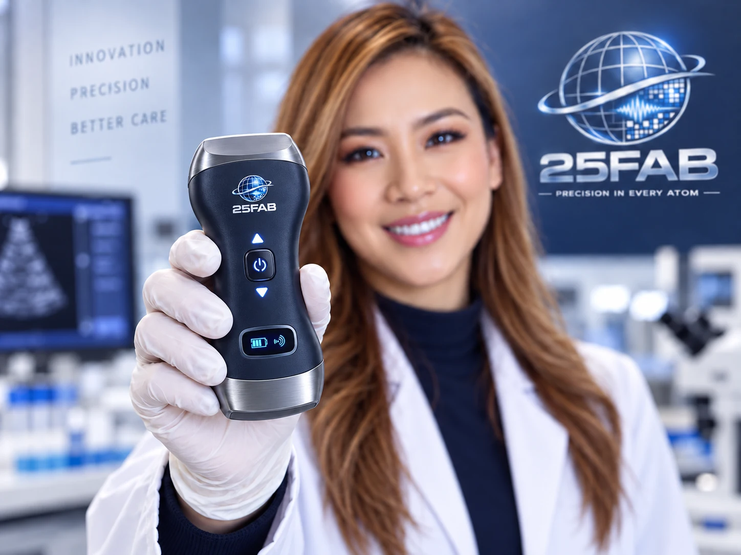
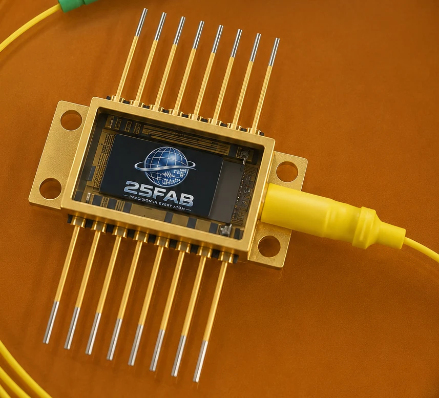
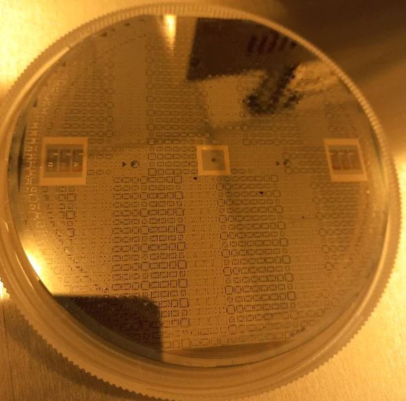
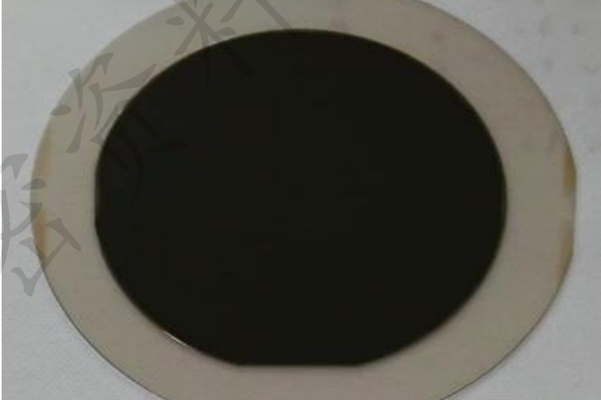
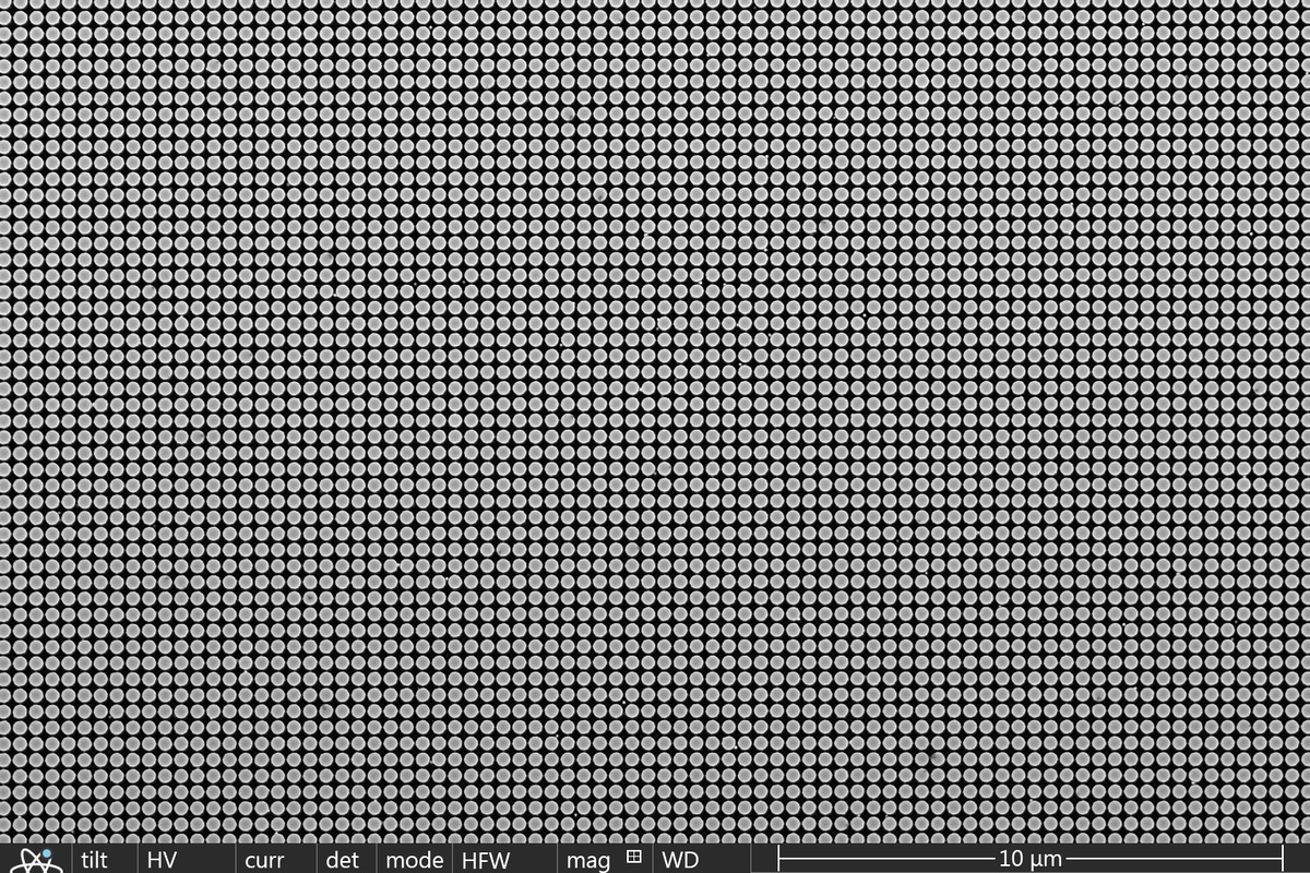
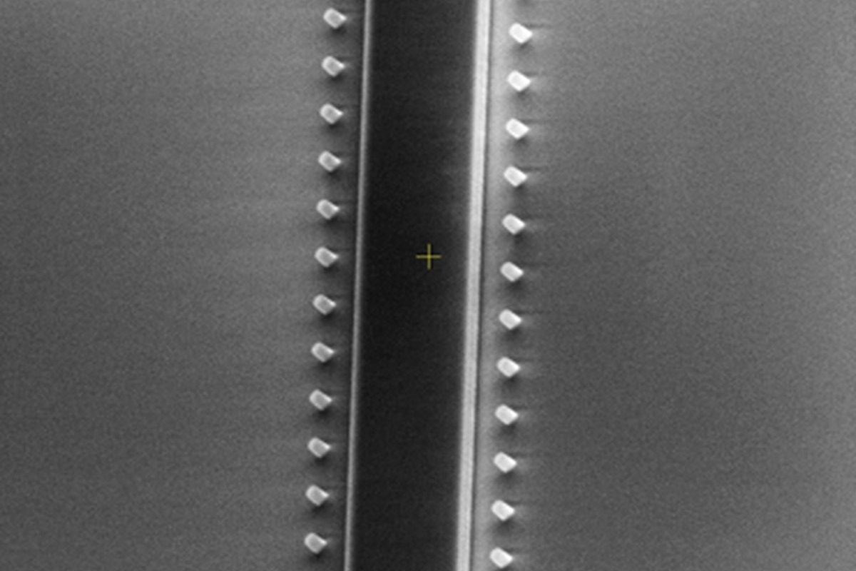
Inside the production
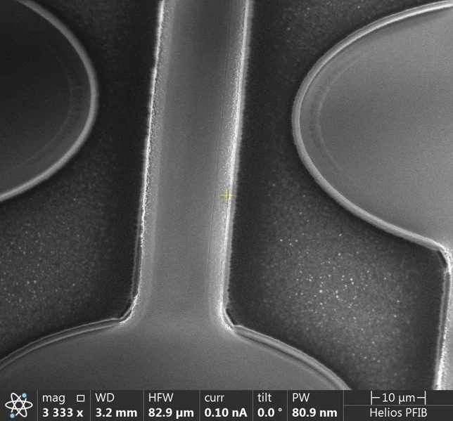
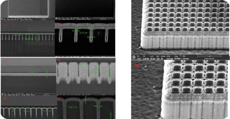

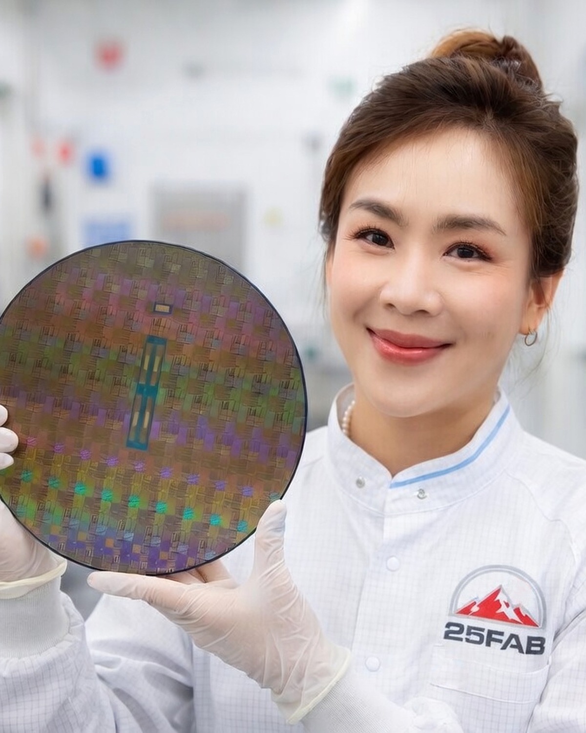
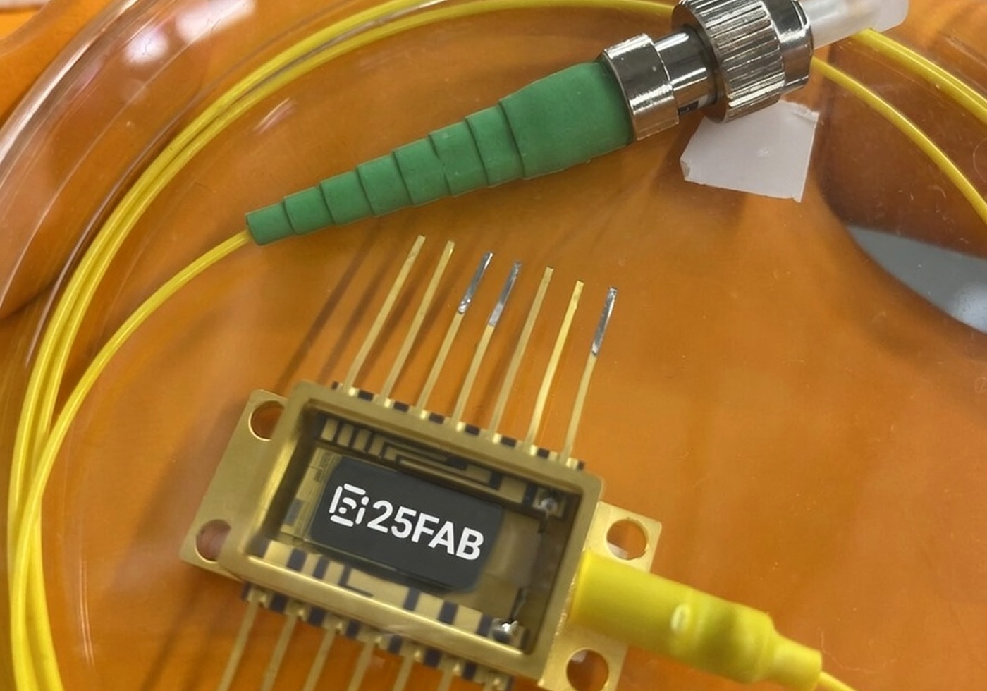
Industries
Processes & technical limits
| Processes | Tolerance | Max. part | Weight | Lot size | Materials |
|---|---|---|---|---|---|
| PMUT manufacturing (piezoelectric ultrasound arrays, large arrays 32 to 1,024+ elements)Additive | – | – | – | – | PZT, AlN, AlScN, BTO-on-Si, Si, SOI |
| Piezoelectric MEMS loudspeakers (wafer-level)Additive | – | – | – | – | PZT, AlN, AlScN |
| Piezoelectric MEMS microphonesAdditive | – | – | – | – | PZT, AlN, AlScN |
| Piezoelectric MEMS micromirrors (1D/2D scanning, beam steering)Additive | – | – | – | – | PZT, AlN, AlScN |
| Piezo-tunable PIC (integrated photonics with piezoelectric actuation, ~1550 nm)Additive | – | – | – | – | Si3N4, SOI, PZT, AlN, AlScN, BTO-on-Si |
| PIC manufacturing (photonic integrated circuits, wafer level)Additive | – | – | – | – | Si3N4, SOI, Ge-on-Si, GeSn, InP, GaAs |
| Metasurface/metalens manufacturing (flat optics)Additive | – | – | – | – | Si3N4, SOI, TiO2, Si |
| SiC platform (semiconductor and MEMS processes for high power/harsh environments)Additive | – | – | – | – | SiC |
| InP platform (photonic/optoelectronic manufacturing)Additive | – | – | – | – | InP, InGaAsP |
| InAs/InGaAs platform (infrared detection, optoelectronics)Additive | – | – | – | – | InAs, InGaAs |
| GaN/GaAs/GeSn/diamond custom platforms (project-specific semiconductor andAdditive | – | – | – | – | GaN, GaAs, Ge-on-Si, GeSn, Diamond, GaN-on-Si, GaN-on-sapphire, AlGaN/GaN |
| Heterogeneous integration (PIC + piezo, PIC + BTO, PMUT-on-ASIC/interposer, III-V-on-photonics)Additive | – | – | – | – | PZT, AlN, AlScN, BTO-on-Si, Si3N4, SOI, InP, GaAs, Si |
| Wafer-level packaging/module integration (OEM module integration, die-to-packaged modules)Assembly | – | – | – | – | Si, Si3N4, SOI, PZT, AlN, InP |
| AI-supported device design / DFM (design reports, FEM/electromagnetic simulation, layout/GDS)Engineering | – | – | – | – | – |
| Quantum photonics & beam-control systems (neutral-atom optics, metasurfaces, tunable PICs)Additive | – | – | – | – | Si3N4, AlN, AlScN, BTO-on-Si |
| MPW / dedicated wafer runs (shared wafer and custom manufacturing)Additive | – | – | – | – | – |
| Wafer-level volume production with quality controlAdditive | – | – | – | – | – |
Additional services