Designs, develops, characterizes and manufactures microsystems and wafer processes from idea to series production.

5microns GmbH
Ilmenau · HeadquartersNew on Amplifa
About 5microns
5microns GmbH from Ilmenau is a technology service provider for microsystems technology specializing in small and medium-sized enterprises as its target group. The company designs, develops, characterizes and manufactures microsystems and wafer processes on behalf of customers – from the idea through design and prototype or small-series production to transfer into high-volume production or the establishment of the customer's own manufacturing resources. The technology portfolio includes lithography (UV lithography, nanoimprint lithography, laser direct writing, resist coating), wet etching (HF/BOE, KOH, metal etchants), dry etching (RIE, DRIE, sputter etching, HF vapor), coating techniques such as PVD, reactive sputtering, LPCVD, PECVD and oxidation, as well as backend processes such as wafer dicing, wire bonding, thermocompression bonding and soldering. For quality assurance, optical and tactile profilometry, SEM and ellipsometry are available. Through access to cleanrooms and its proximity to TU Ilmenau, the company serves customers from microsystems technology, MEMS and photonics, supporting both first-time users and specialists throughout the entire product development cycle.
- Site
- Ilmenau
- Processes
- UV lithography, Nanoimprint lithography (UV-NIL), Laser direct writing, Resist coating, Wet etching with hydrofluoric acid (HF or BOE), Wet etching with KOH, Wet etching with metal etchant, Dry etching RIE (reactive ion etching)
- Materials
- UV Lithography, Nanoimprint Lithography (UV-NIL), Laser Direct Writing, Wet Etching (HF/BOE, KOH, Metal Etchants), Dry Etching (RIE, DRIE, Sputter Etching, HF Vapor), PVD (Sputtering, Evaporation, Reactive Sputtering), LPCVD / PECVD (CCP & ICP), Oxidation
- Certificates
- Optical and tactile profilometry, Scanning electron microscopy (SEM), Ellipsometry, ISO 9001
- Industries
- Microsystems technology, MEMS, Optics/Photonics, Small and medium-sized enterprises, Small and medium-sized enterprises / Microsystems technology, Optics/Photonics (implied via OptoNet network)
- 01
Consulting throughout the entire product development cycle
- 02
Design of microsystems
- 03
Lithography
- 04
Etching
- 05
Coating
- 06
Backend (wafer dicing, bonding, soldering)
- 07
Characterization and metrology
- 08
Prototype and small-series production
- 09
Transfer into high-volume production
Microtechnologies and Processes
UV Lithography
Structuring of photoresists for microsystem processes.
Nanoimprint Lithography (UV-NIL)
Nanopatterning of large areas without optical exposure.
Laser Direct Writing
Maskless direct structuring on wafers.
Wet Etching (HF/BOE, KOH, Metal Etchants)
Wet-chemical etching processes for silicon, oxides and metal layers.
Dry Etching (RIE, DRIE, Sputter Etching, HF Vapor)
Plasma-based etching processes for anisotropic and deep structures.
PVD (Sputtering, Evaporation, Reactive Sputtering)
Deposition of metallic and dielectric thin films.
LPCVD / PECVD (CCP & ICP)
Deposition of layers such as nitride, oxide or polysilicon.
Oxidation
Thermal oxide layer growth on silicon wafers.
Backend (Wafer Dicing, Wire Bonding, Thermocompression Bonding, Soldering)
Chip singulation, contact placement and joining processes.
Locations
Ilmenau
DEHeadquarters with manufacturing and metrology
- Lot size
- Prototype to small series
- Materials
- Silicon wafer processes, thin films
- Cleanroom access
- Profilometry
- SEM
- Ellipsometry
Components and Microsystems
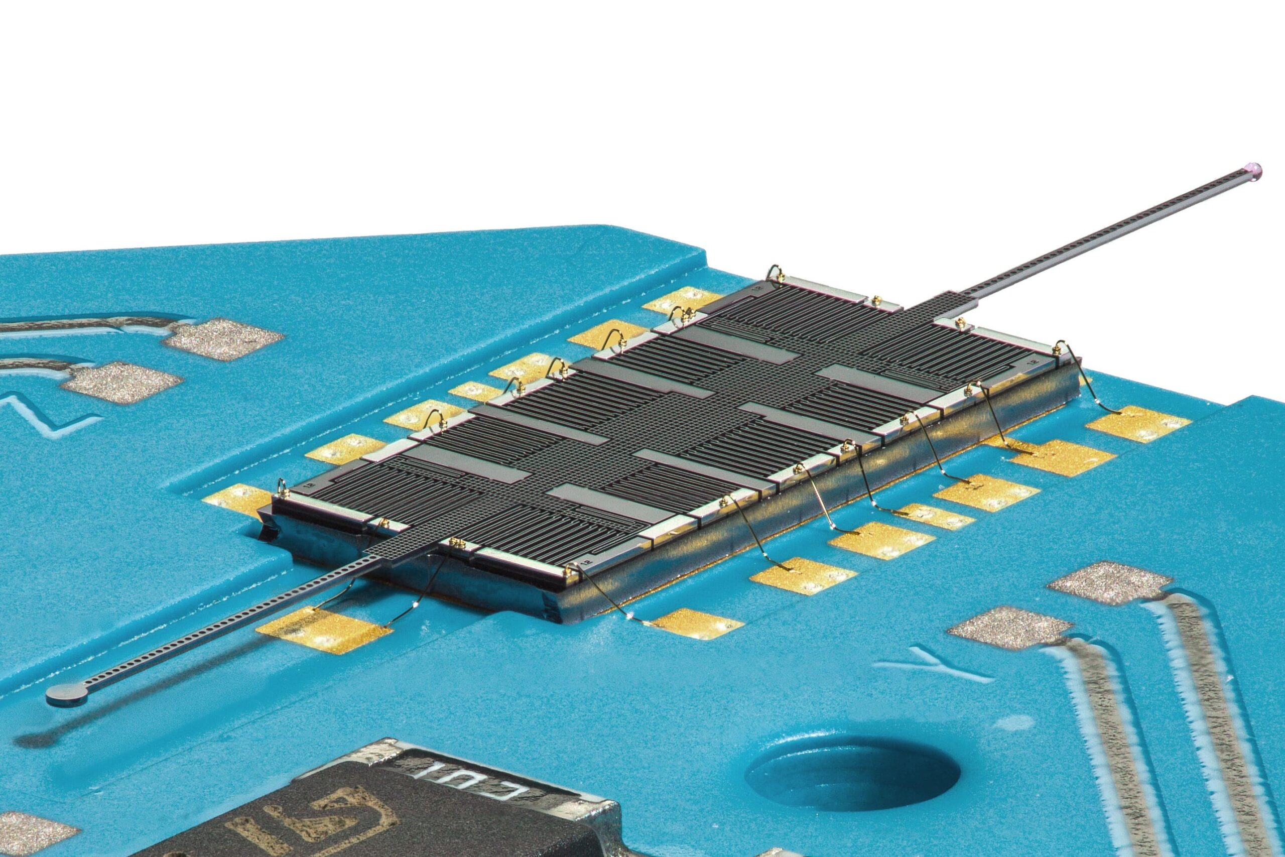
Inside the production
Industries
Processes & technical limits
| Processes | Tolerance | Max. part | Weight | Lot size | Materials |
|---|---|---|---|---|---|
| UV lithographySurface | – | – | – | Prototype – Small series | – |
| Nanoimprint lithography (UV-NIL)Surface | – | – | – | – | – |
| Laser direct writingSurface | – | – | – | – | – |
| Resist coatingSurface | – | – | – | – | – |
| Wet etching with hydrofluoric acid (HF or BOE)Surface | – | – | – | – | – |
| Wet etching with KOHSurface | – | – | – | – | – |
| Wet etching with metal etchantSurface | – | – | – | – | – |
| Dry etching RIE (reactive ion etching)Surface | – | – | – | – | – |
| Dry etching DRIE (deep reactive ion etching)Surface | – | – | – | – | – |
| Sputter etchingSurface | – | – | – | – | – |
| HF vapor etchingSurface | – | – | – | – | – |
| PVD coating (sputtering and evaporation)Surface | – | – | – | – | – |
| Reactive sputteringSurface | – | – | – | – | – |
| LPCVD coatingSurface | – | – | – | – | – |
| PECVD coating (CCP & ICP)Surface | – | – | – | – | – |
| OxidationHeat treatment | – | – | – | – | – |
| Wafer dicingMachining | – | – | – | – | – |
| Wire bondingJoining | – | – | – | – | – |
| Thermocompression bondingJoining | – | – | – | – | – |
| SolderingJoining | – | – | – | – | – |
| Optical and tactile profilometryTesting | – | – | – | – | – |
| SEM (scanning electron microscopy)Testing | – | – | – | – | – |
| EllipsometryTesting | – | – | – | – | – |
| Design of microsystemsEngineering | – | – | – | – | – |
| Development and characterization of MEMS prototypesEngineering | – | – | – | – | – |
| Microfabrication and wafer processingSurface | – | – | – | Prototype – Small series | – |
| Consulting throughout the entire product development cycle (from idea to series)Engineering | – | – | – | – | – |
| Transfer into high-volume production / establishment of own manufacturing resourcesEngineering | – | – | – | – | – |
Additional services
Reference customers
Quality and Metrology
For characterization and testing, optical and tactile profilometry, scanning electron microscopy (SEM) and ellipsometry are available.
| Evidence | Ilmenau |
|---|---|
| Optical and tactile profilometry | |
| Scanning electron microscopy (SEM) | |
| Ellipsometry | |
| ISO 9001 |