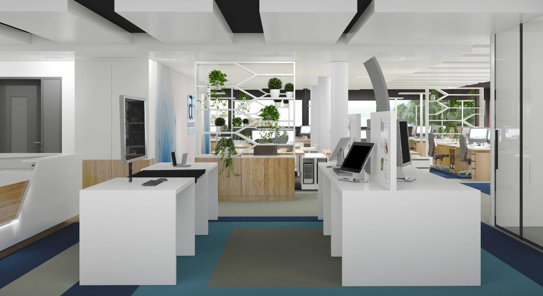
Fabless design house for mixed-signal ICs and touch modules for medical technology, aerospace and industry

Advanced Silicon SA
Lausanne (Switzerland)New on Amplifa
About Advanced Silicon
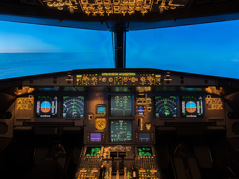
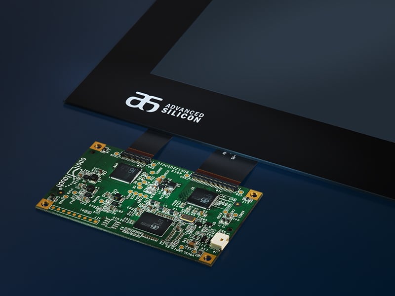
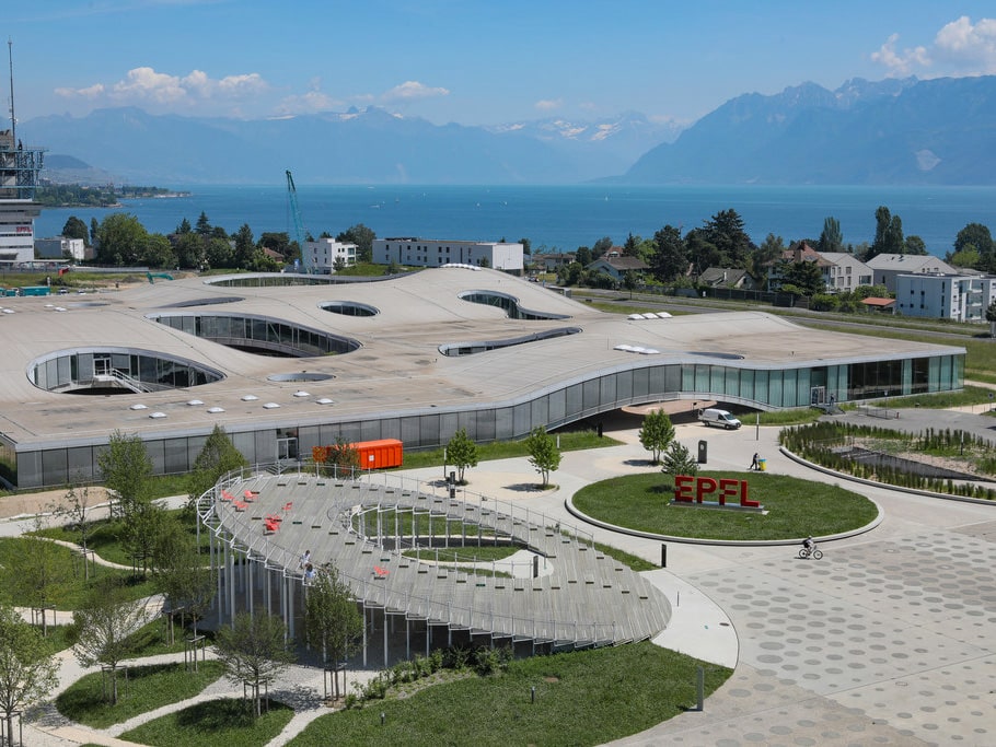
Advanced Silicon SA is a fabless design company based in Lausanne that develops analog, mixed-signal and high-voltage integrated circuits (ASSPs and ASICs) and delivers them as turnkey solutions through to series production. The focus is on ICs for photonic detectors in medical X-ray panels, driver and timing ICs for TFT cockpit displays in avionics, and touch ICs and capacitive touch modules for industrial applications from 7 to 84 inches. The company was incubated in 2000 at the École Polytechnique Fédérale de Lausanne (EPFL) and continuously invests in its own R&D roadmap as well as joint research projects with EPFL. Manufacturing takes place via an established production network, among others with partner Weida Hitech in Taiwan; Advanced Silicon covers the entire value chain from SOC design through foundry, reliability qualification, assembly & test to production and logistics. For touch modules, sensor stacks made of glass (GG, GF2, OGS) and sensor materials such as silver nano-wire, ITO and metal mesh are used. Customers come from the medical technology, aerospace, industrial and consumer electronics sectors.
- Site
- Lausanne
- Processes
- ASIC development (turnkey: SOC design, foundry, reliability qualification, assembly & test,, Touch module development (turnkey: SOC design, touch module, qualification, testing, production &, P-CAP touch panel development (design and optimization of diamond pixel patterns, sensor stacks, IC design for mixed-signal and high-voltage integrated circuits (ASSPs, ASICs), ASIC development (turnkey: SOC design, foundry, qualification, assembly & test, production &, Touch module development (turnkey), PCAP touch systems, IC design for sensing, high voltage and microcontrollers (RISC-V)
- Materials
- Silicon (silicon), Silver Nano-Wire (SNW), Indium Tin Oxide (ITO), Metal Mesh (MM), Glass (glass-glass, glass-film, one-glass-sensor, cover glass), Silicon (mixed-signal ICs), Turnkey ASIC development, P-CAP touch panel development
- Certificates
- ISO 9001:2015, HSF policy (RoHS, REACH, halogen-free)
- Founded
- 2000
- Industries
- Medical technology (photon detector / X-ray), Aerospace / avionics, Industry (touch screens, HMI), Consumer electronics
- 01
SOC design
- 02
Foundry
- 03
Reliability qualification
- 04
Assembly & test
- 05
Production & logistics
Materials & Processes
Silicon (mixed-signal ICs)
Monolithic circuits with massively parallel signal processing of up to 1024 channels for sensing, high-voltage drivers and microcontrollers.
Turnkey ASIC development
Comprehensive development from specification through foundry to qualification, assembly, test and logistics.
P-CAP touch panel development
Design and optimization of diamond pixel patterns, sensor stacks (GG, GF2, OGS) as well as cover glass coating and shaping up to 84".
Silver Nano-Wire (SNW)
Sensor material for projected-capacitive touch panels with high conductivity.
Indium Tin Oxide (ITO)
Standard transparent electrode material for capacitive touch sensors.
Metal Mesh (MM)
Sensor material for large-format touch panels with low sheet resistance.
Glass (GG, GF2, OGS)
Sensor stack structures glass-glass, glass-film and one-glass-sensor including AR, AG and AS cover glass coating.
Special microcontrollers (RISC-V)
32-bit RISC-V architecture with coprocessors for image processing and machine learning algorithms.
Locations
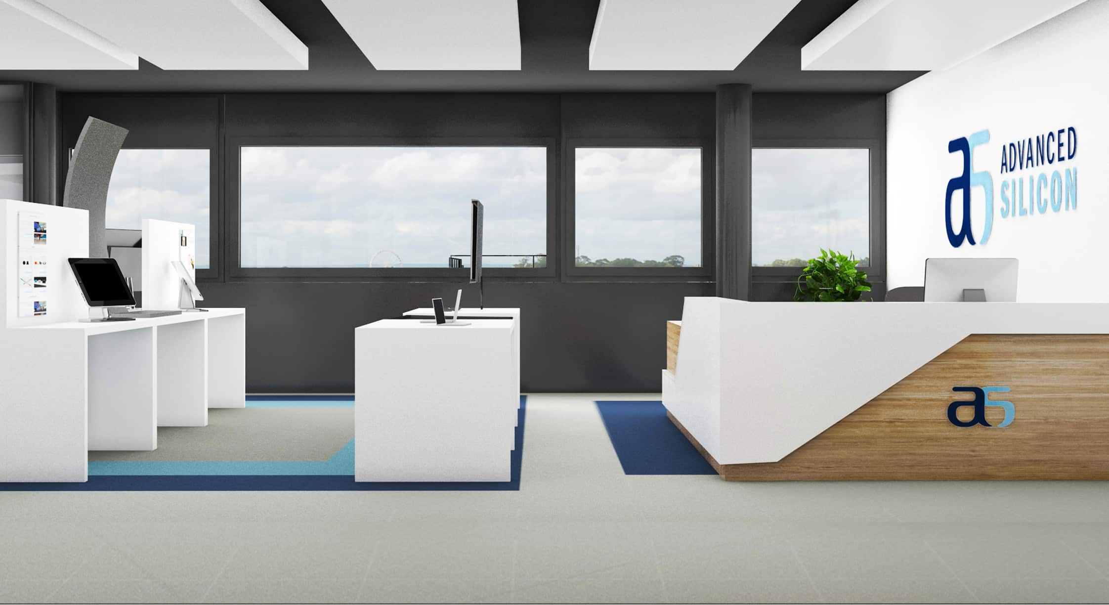
Lausanne
CHHeadquarters and development (fabless)
- Materials
- Silicon, glass, SNW, ITO, metal mesh
Products & Components
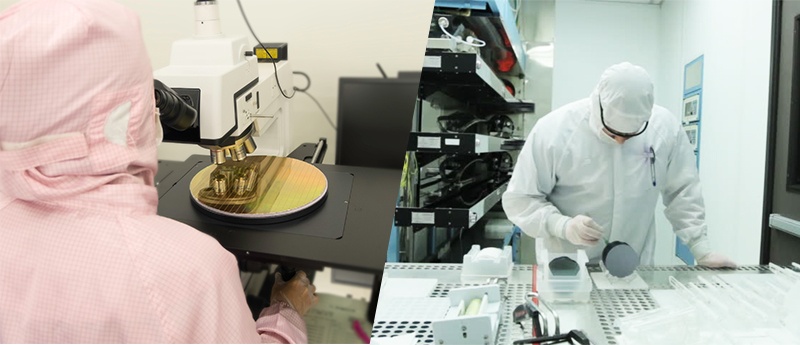

Inside the production

Industries
Processes & technical limits
| Processes | Tolerance | Max. part | Weight | Lot size | Materials |
|---|---|---|---|---|---|
| ASIC development (turnkey: SOC design, foundry, reliability qualification, assembly & test,Engineering | – | – | – | – | Silicon |
| Touch module development (turnkey: SOC design, touch module, qualification, testing, production &Engineering | – | – | – | – | – |
| P-CAP touch panel development (design and optimization of diamond pixel patterns, sensor stacksEngineering | – | 84" touch panel size | – | – | Glass, Silver Nano-Wire (SNW), Indium Tin Oxide (ITO), Metal Mesh (MM) |
| IC design for mixed-signal and high-voltage integrated circuits (ASSPs, ASICs)Engineering | – | – | – | – | Silicon |
Additional services
Reference customers
Quality
The quality management system introduced in 2007 is certified to ISO 9001:2015 (SQS/IQNET, reg. no. CH-34070). In-line screening methods on all components support the zero-defect policy; complaints and internal issues are handled via the 8D process.
| Evidence | Lausanne |
|---|---|
| ISO 9001:2015 | |
| HSF policy (RoHS, REACH, halogen-free) |
History
- 2000
Incubation at EPFL (Swiss Federal Institute of Technology) with a focus on ICs for digital flat-panel imagers, high-voltage drivers and ultra-low-noise sensing ICs.
- 2007
Establishment of the quality management system for ISO-9001 certification.
- aktuell
Spin-off of the system electronics division into the unit Elix Systems; joint venture with ADIS SA for computer vision systems for hospitals based on ATICS technology.