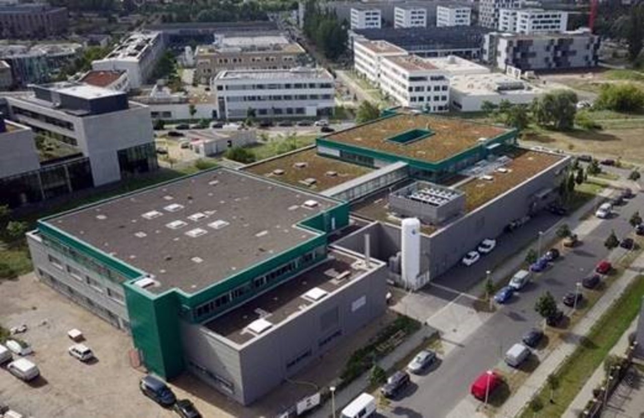
Development, industrialization and manufacturing of complex micro- and optoelectronic modules in cleanroom up to ISO 5.

AEMtec GmbH
Berlin · Dresden · Boston (USA)New on Amplifa
About AEMtec
AEMtec GmbH, headquartered at the science and technology hub Berlin-Adlershof, specializes in the development, industrialization and production of complex micro- and optoelectronic modules through to complete systems. The technology portfolio covers Wafer Back-End Services (UBM, solder balling, wafer dicing), chip and wire bonding, flip-chip, SMT assembly, opto-packaging, fan-out wafer-level packaging, 3D integration and system integration through to customer-specific test and automation solutions. Production takes place in cleanrooms of ISO classes 5 to 8, with placement accuracies down to ±0.5 µm on high-precision die bonders. Materials processed include silicon wafers, glass, ceramics, FR4, rigid and rigid-flex printed circuit boards, and plastics such as LCP and polyimide. Customer groups come from medical and biotechnology, AI and communications, industrial and automation, semiconductors, as well as aerospace and defense. In addition to Berlin, AEMtec operates sites in Dresden (aSpect Systems) and a Tech Center in Boston.
- Site
- Berlin
- Processes
- Wafer Back-End Services, UBM (Under Bump Metallization) / ENB - Electroless Ni-Au Plating, Solder Balling (Ball/Bump Forming, Ball Drop, Printing Processes), Wafer Dicing, Wafer Grinding (in cooperation with partners), Wafer Testing (in cooperation with partners), SMT - Surface Mount Technology (stencil printing, dispensing, SMD placement, reflow soldering, AOI), Chip on Board (CoB) / Chip on Glass (CoG) - Chip & Wire Bonding
- Materials
- Silicon, Glass, FR4, Standard printed circuit boards (rigid), Rigid-flex printed circuit boards, Film, Ceramics, IMS
- Certificates
- ISO 9001:2015, ISO 13485:2016, ISO 14001:2015, SBTi Science-Based Targets (Net-Zero/Near-Term), SBTi-validated climate targets, Cleanroom ISO 5
- Employees
- >300 (worldwide,
- Industries
- Medical & Biotechnology, AI & Communications, Industry & Automation, Semiconductors, Aerospace & Defense
- 01
Design & Development
- 02
Prototyping (NPI)
- 03
Industrialization & Qualification
- 04
Wafer Back-End Services
- 05
Chip/Wire Bonding, Flip-Chip, SMT, Opto-Packaging
- 06
Testing & Test System Development
- 07
Series Production
- 08
Supply Chain Management & After Sales Services
Materials & Processes
Silicon (wafers, chips)
Base material for wafer back-end services, flip-chip and 3D integration.
UBM / Electroless Ni-Au Plating
Electrolessly deposited under-bump metallization (NiAu, NiPdAu) using a Fraunhofer IZM process, maskless.
Aluminium
Pad metallization and bonding wires for chip and wire bonding.
Copper
Pad metallization for UBM processes.
Gold
Bonding wires and bump metallization (NiAu, NiPdAu).
Lead-free, lead-containing and low-temperature solders
Solders for solder balling (50–400 µm ball diameter) and reflow soldering.
Printed circuit boards (rigid, rigid-flex), film, ceramics, IMS
Substrates for SMT assembly up to 75 × 75 mm or 50 × 150 mm.
LCP, polyimide, epoxy glass fabric
High-strength substrate materials for SMT and miniaturization.
Epoxies, silicones, acrylates
Encapsulation materials for opto-packaging, 1- and 2-component, thermally or UV curing.
Sites
Berlin
DEHeadquarters, development & cleanroom production ISO 5–8
- Part weight / size
- Wafers up to 300 mm (12 inch)
- Lot size
- Prototype to series
- Materials
- Si, glass, ceramics, FR4, solders
- UBM line (electroless plating, 2024)
- Solder balling systems (manual and fully automated)
- Fully automated precision saws (wafer dicing)
- SMD placement machines
- High-precision die bonders (±0.5 µm)
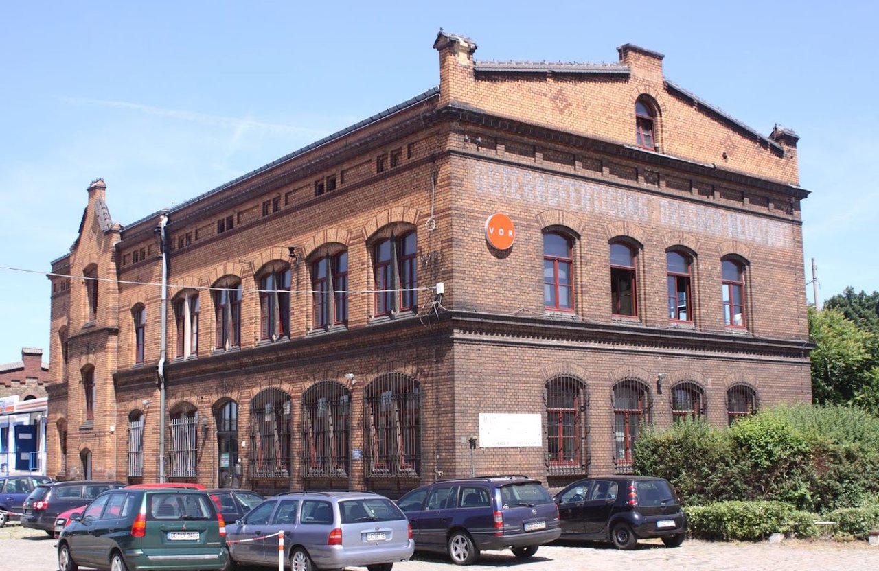
Dresden
DEaSpect Systems GmbH – Custom Test & Automation
- Custom Test & Automation Solutions
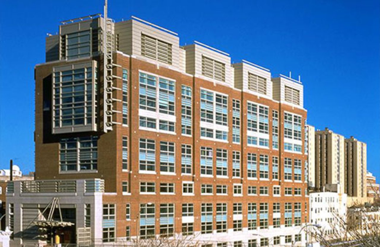
Boston (USA)
USAEMtec USA Inc. – US Tech Center: consulting, rapid prototyping
- Lot size
- Prototype
- Rapid prototyping lab
Components & Modules
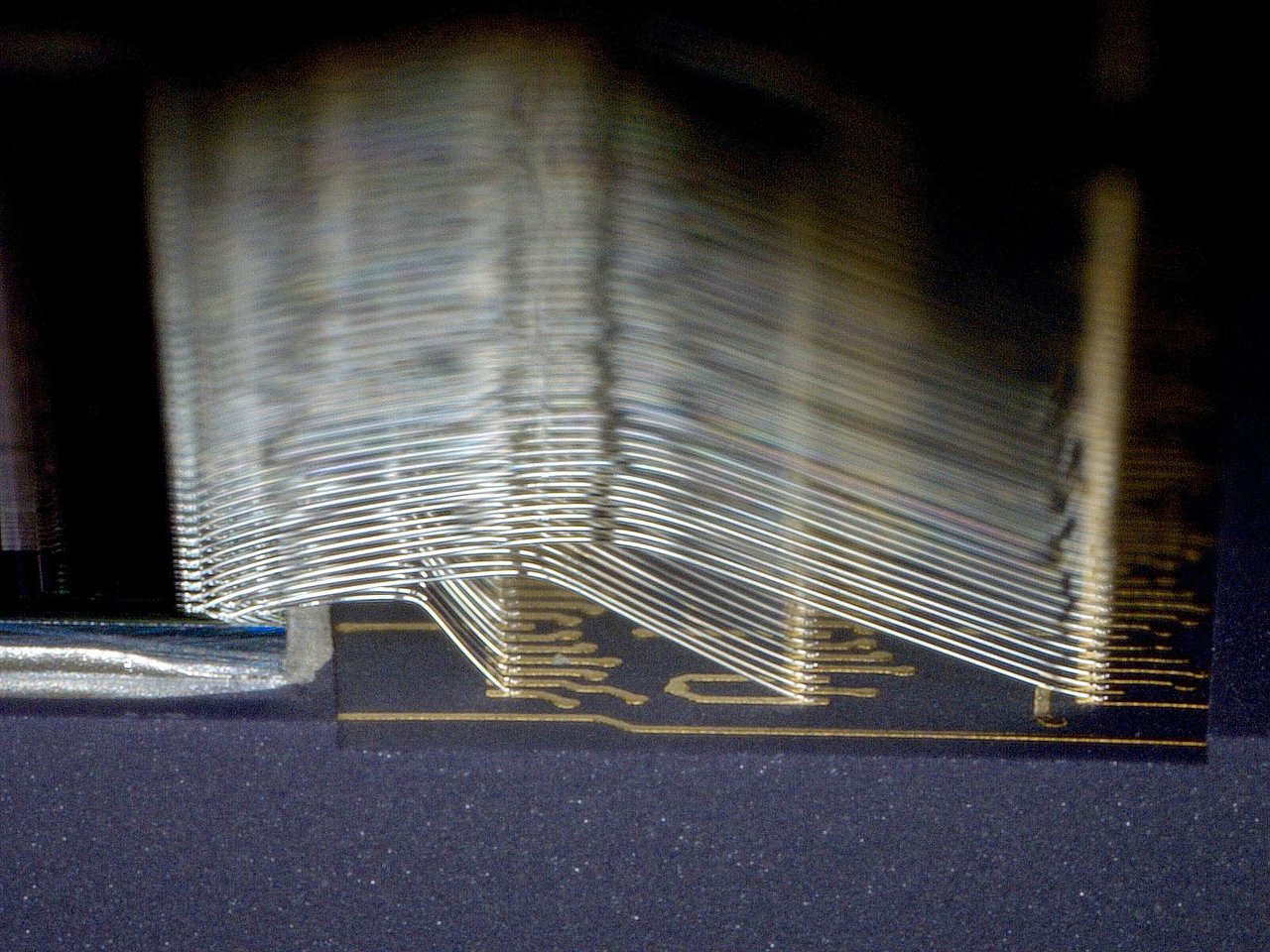
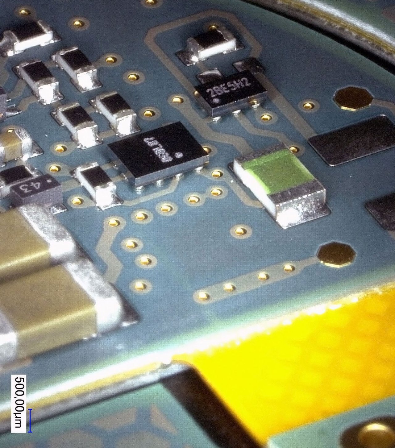
Inside the production
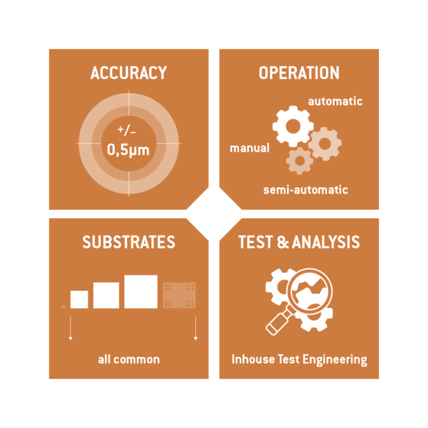

Industries
Processes & technical limits
| Processes | Tolerance | Max. part | Weight | Lot size | Materials |
|---|---|---|---|---|---|
| Wafer Back-End ServicesSemiconductor Packaging | – | 300 mm (12-inch wafer) | – | – | Silicon, Glass, FR4 |
| UBM (Under Bump Metallization) / ENB - Electroless Ni-Au PlatingSemiconductor Packaging | – | – | Wafer thickness > 200µm | – | Al (pad metallization), Cu (pad metallization), NiAu (bump), NiPdAu (bump) |
| Solder Balling (Ball/Bump Forming, Ball Drop, Printing Processes)Semiconductor Packaging | – | 6 to 12-inch wafers | – | – | SAC solder, Solders of all available alloys |
| Wafer DicingSemiconductor Packaging | – | 300mm (12 inch) | – | – | Silicon, Glass, FR4, MEMS structures |
| Wafer Grinding (in cooperation with partners)Semiconductor Packaging | – | – | – | – | Si, Glass |
| Wafer Testing (in cooperation with partners)Testing | – | – | – | – | Silicon wafers |
| SMT - Surface Mount Technology (stencil printing, dispensing, SMD placement, reflow soldering, AOI)Joining | – | 50 x 150mm × 75 x 75mm | – | – | Standard printed circuit boards (rigid, rigid-flex), Film, Ceramics, Silicon wafers, Glass, IMS, LCP, Polyimide, Epoxy glass fabric |
| Chip on Board (CoB) / Chip on Glass (CoG) - Chip & Wire BondingJoining | +/- 0.5µm | – | – | – | Silicon, Gold (bonding wires), Aluminium (bonding wires) |
| Wire Bonding (gold and aluminium wire bonding)Joining | – | – | – | – | Gold, Aluminium |
| Flip-Chip SolderingJoining | – | – | – | – | Silicon, TSV chips, Solders |
| Flip-Chip Isotropic Bonding (ICA)Joining | – | – | – | – | Silicon |
| Flip-Chip Anisotropic Bonding (ACA/ACF)Joining | – | – | – | – | Silicon |
| Flip-Chip Thermosonic / Thermocompression / UltrasonicJoining | – | – | – | – | Silicon |
| TSV (Through Silicon Via) ProcessingSemiconductor Packaging | – | – | – | – | Silicon |
| Opto-Packaging (active and passive alignment)Joining | +/- 0.5µm | – | – | – | Laser diodes, PIN diodes, Glass, Ceramics |
| Lens Array Alignment (active alignment of optics)Assembly | – | – | – | – | Glass, Optical components |
| Optical Encapsulation (dispensing/jetting nano- to milliliter, 1- and 2-component, thermally/UVPlastics | – | – | – | – | Epoxies, Silicones, Acrylates |
| Encapsulation (globtop, dam & fill)Plastics | – | – | – | – | Epoxies, Silicones |
| Fan-Out Wafer-Level Packaging (FOWLP, Compression Molding, RDL)Semiconductor Packaging | – | – | – | – | Silicon, Mold material, Thin-film redistribution |
| Custom Test and Automation Solutions (wafer probing, end-of-line testing, AOI, active alignment)Testing | – | – | – | – | – |
| Design, Development and Industrialization (engineering, NPI, prototyping)Engineering | – | – | – | – | – |
| Qualification/Reliability Laboratory (temperature shock, climate, burn-in, mechanical analysis)Testing | – | – | – | – | – |
| Product-Specific Testing (AOI, ICT, FCT, burn-in)Testing | – | – | – | – | – |
| System Integration / SiP (multi-chip modules in mixed technologies)Assembly | – | – | – | – | Standard printed circuit boards, Ceramics, Silicon wafers, Glass, IMS |
| 3D IntegrationSemiconductor Packaging | – | – | – | – | Silicon |
| Rapid Prototyping (US Tech Center Boston)Engineering | – | – | – | – | – |
| Reflow SolderingJoining | – | – | – | – | lead-free and lead-containing solders, low-temperature solders |
5 Anlagen & Maschinen
| Machine | Manufacturer / model | Quantity | Working area | Year built | Site |
|---|---|---|---|---|---|
| UBM line (electroless plating) | – | – | – | 2024 | Berlin |
| Solder balling systems (manual and fully automated) | – | – | 6 to 12-inch wafers, ball diameter 50–400µm | – | Berlin |
| Fully automated precision saws (wafer dicing) | – | – | up to 300mm (12 inch) | – | Berlin |
| SMD placement machines | – | – | – | – | Berlin |
| High-precision die bonders | – | – | Placement accuracy down to 0.5µm XY, rotation angle 3.5 µrad | – | Berlin |
Additional services
Reference customers
Quality & Certification
Certified quality management according to ISO 9001 and ISO 13485 with an in-house reliability laboratory (temperature shock, climate, burn-in, mechanical analysis), product-specific tests (AOI, ICT, FCT, burn-in), SPC, database-supported traceability and yield management. Environmental management is certified according to ISO 14001; the CO₂ reduction targets have been validated by SBTi.
| Evidence | Berlin |
|---|---|
| ISO 9001:2015 | |
| ISO 13485:2016 | |
| ISO 14001:2015 | |
| SBTi-validated climate targets | |
| Cleanroom ISO 5 |
History
- 2003
Robert Giertz as working student/thesis student at AEMtec
- 2007
Thomas John supports AEMtec's sales activities
- 2009
Robert Giertz returns to AEMtec
- 2010
Thomas John and Jan Trommershausen take responsibility for sales and management respectively
- 2012
Robert Giertz heads the Engineering division
- 2018
Robert Giertz becomes CTO
- 2019
Thomas John becomes Managing Director; build-up of Wafer Back-End Services
- 2021
Expansion of the company building in Berlin
- 2024
New UBM system in-house (electroless UBM transferred from Fraunhofer IZM)
- 2025
Robert Giertz becomes Managing Director; SBTi target validation in October 2025
- 2026
AEMtec and Micross sign agreement – AEMtec becomes part of Micross