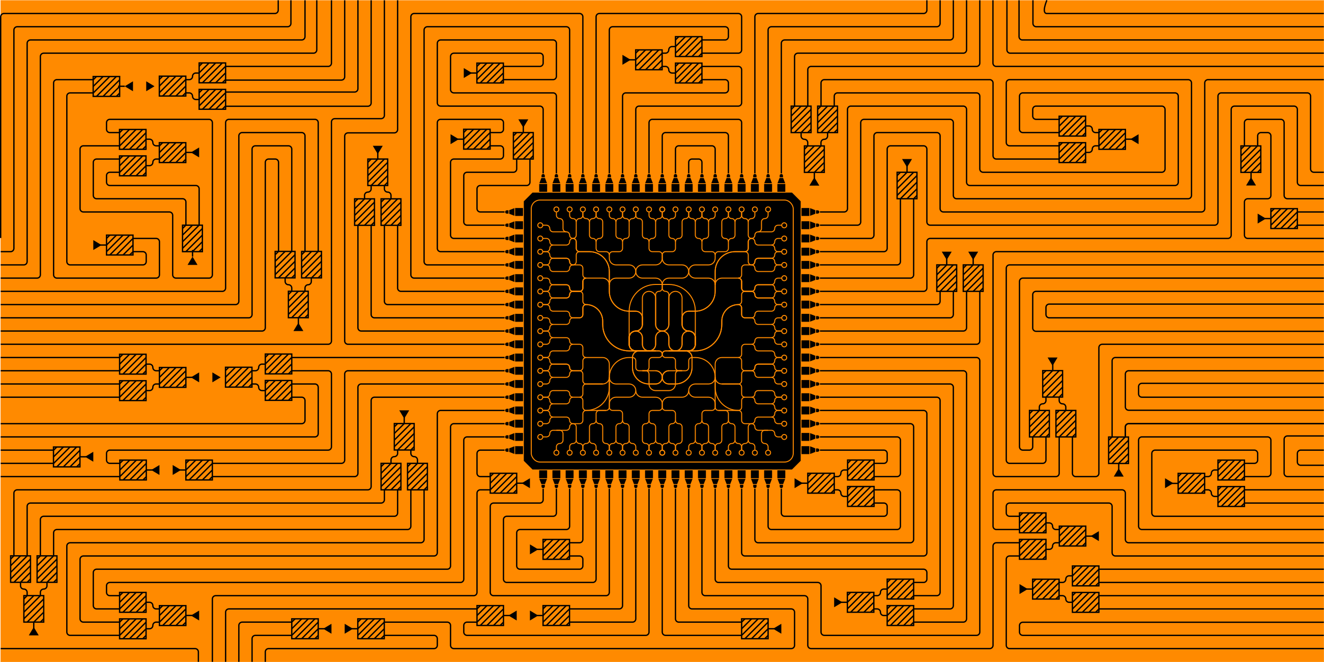
Development of all-optical processors (RPU/XPU) based on photonic integrated circuits for AI, reasoning and optimization

Akhetonics GmbH
Berlin (Akazienstr. 3a, 10823) · Munich (Bunzlauer Str. 7, 80992)New on Amplifa
About Akhetonics
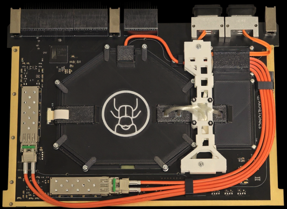
Akhetonics is a design and technology company based in Berlin and develops all-optical processors — the RPU (Reasoning Processing Unit) or Cross-Domain Processor (XPU) — based on photonic integrated circuits (PIC). The core of the technology is in-house developed optical nonlinearities and waveguide-based computing building blocks made from material combinations such as silicon nitride (SiN) and silicon oxide (SiO2), complemented by III-V and 2D materials. The chips are manufactured at external partner foundries on established semiconductor nodes (90 nm, 130 nm, 250 nm) with reference to a European supply chain. Circuit development uses a proprietary VLSI design tool (AtetDesigner) with an RTL-to-GDSII flow. Target industries are AI and high performance computing at edge and cloud, automated reasoning, operations research and quantum-optical applications. For corporate customers, a demo processor is provided for benchmarking of use cases.
- Site
- Berlin
- Processes
- Development of all-optical processors (RPU/XPU), Photonic Integrated Circuits Design, Optical computing (digital, analog, quantum), Custom ISA / software development, Demo processor for customer benchmarking
- Materials
- Silicon nitride, Silicon oxide, III-V and 2D materials
- Industries
- AI / High Performance Computing, Edge & Cloud Computing, Quantum Computing, Operations Research
- 01
System and architecture development
- 02
Photonic design & simulation
- 03
PIC layout (AtetDesigner, RTL-to-GDSII)
- 04
Manufacturing at partner foundries (mature nodes)
- 05
Chip characterization in our own Photonics Lab
- 06
Benchmarking / demo processor for customers
- 07
Software development with custom ISA
Technologies & Material Platforms
Silicon nitride
Waveguide material of the PIC platform; guides light from the visible to the near-infrared range with virtually no loss.
Silicon oxide
Together with SiN, forms the refractive index contrast for micrometer-scale optical waveguides.
III-V and 2D materials
Enable optical nonlinearities in the PIC for all-optical switches, memories and computing building blocks; optimized jointly with partner foundries.
Locations
Berlin
DEHeadquarters and registered office (Akazienstr. 3a, 10823)
- Materials
- SiN, SiO2, III-V/2D
- AtetDesigner (photonic VLSI, RTL-to-GDSII)
- Photonics Lab for chip characterization
Munich
DELocation (Bunzlauer Str. 7, 80992)
Products & Components
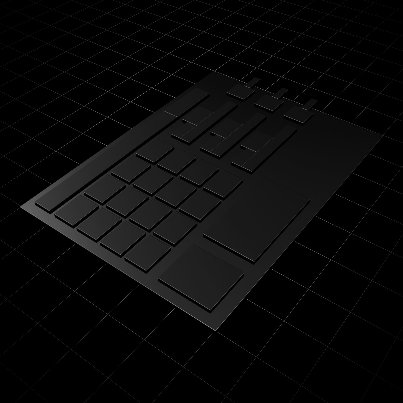
Inside the production
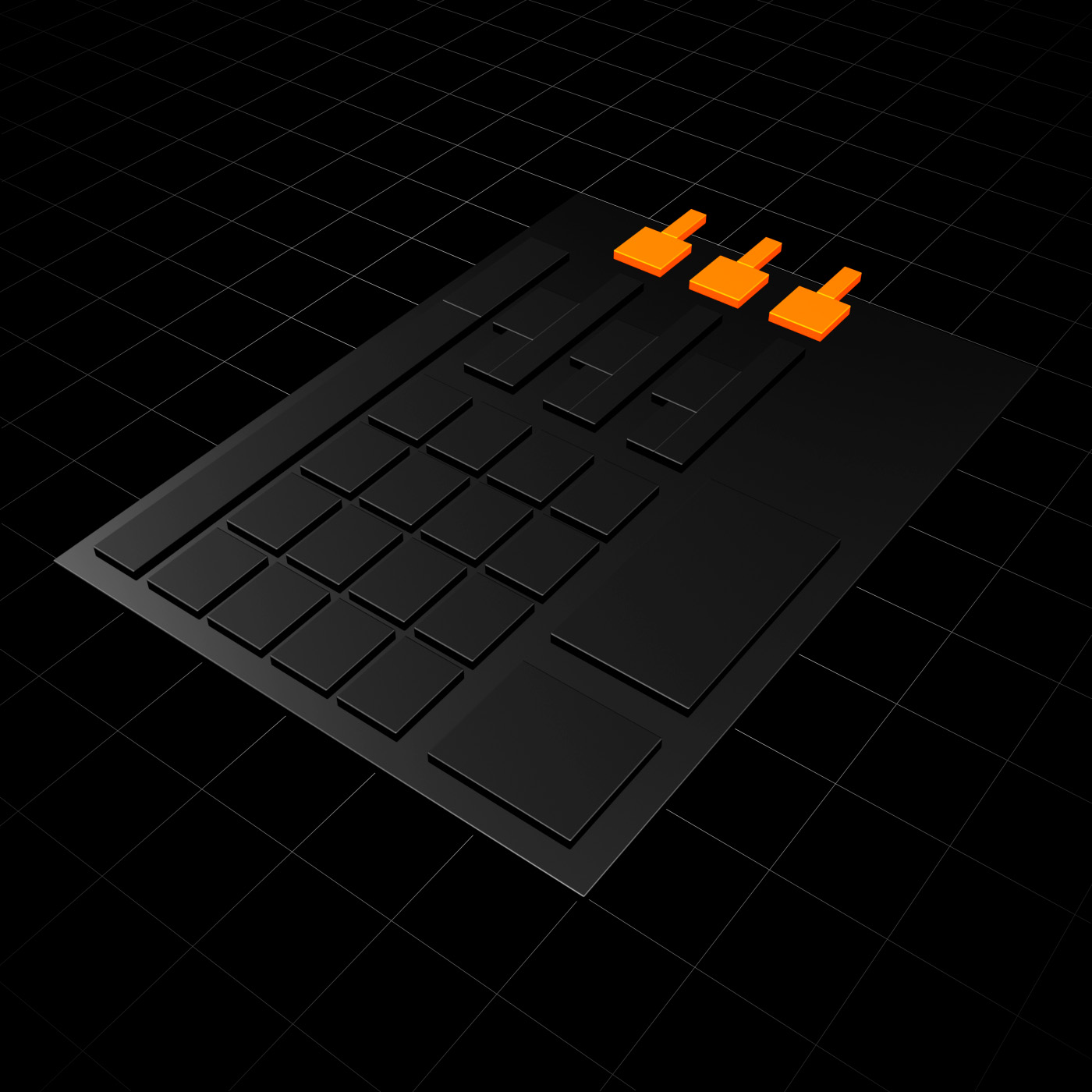


Industries
Additional services