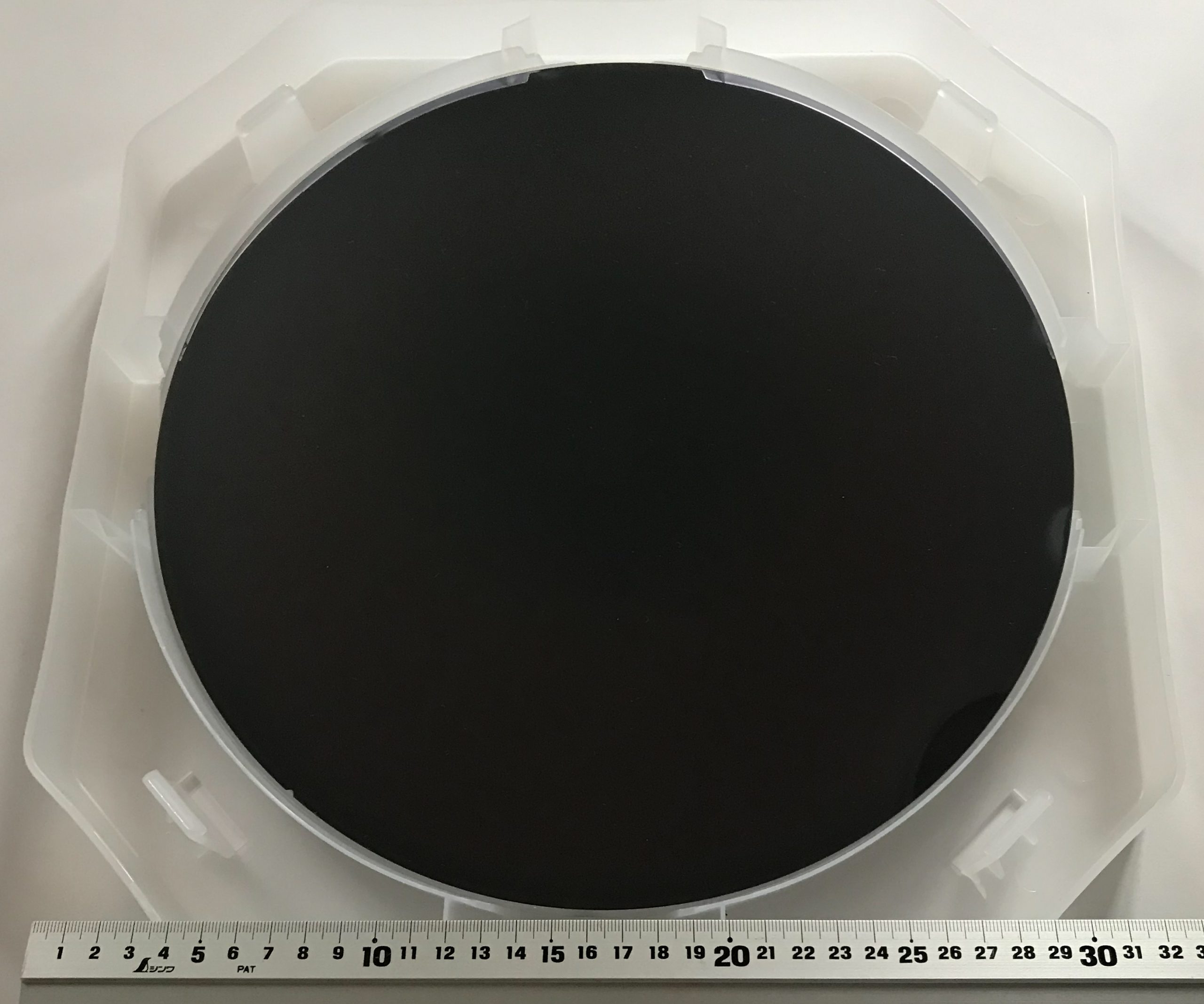
Develops GaN-on-Silicon epiwafers for MicroLED displays and optical interconnects in 200 mm and 300 mm.
ALLOS Semiconductors GmbH
DresdenNew on Amplifa
About ALLOS Semiconductors
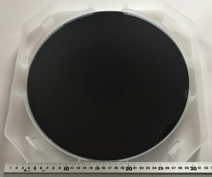
ALLOS Semiconductors is a private high-tech company founded in 2014 and headquartered in Dresden, and is a supplier of GaN-on-Silicon epiwafers (gallium nitride on silicon) for MicroLED applications. The materials serve two high-growth markets: MicroLED-based optical interconnects for AI computing, and MicroLED displays as visual interfaces to AI systems, especially AR displays. ALLOS operates as a fabless company and uses a global network of qualified contract manufacturers and specialized suppliers; this enables flexible scaling including onshoring and on-site manufacturing. All epiwafers are fully silicon-fab compatible and available in 200 mm and 300 mm wafer diameters, allowing MicroLED manufacturing in existing silicon fabs including advanced wafer-to-wafer bonding technologies. As early as 2020, ALLOS demonstrated a 300 mm LED epiwafer as the first company worldwide. The products are protected by an IP portfolio of around 100 patents.
- Site
- Dresden
- Processes
- Manufacture of GaN-on-Silicon epiwafers (epitaxy wafers for MicroLEDs), Supply of epiwafers in 200 mm and 300 mm wafer diameters (fabless via contract manufacturers), Fabless production via a network of qualified contract manufacturers, Onshoring / on-site manufacturing, IP portfolio (approx. 100 patents)
- Materials
- GaN-on-Silicon (gallium nitride on silicon, epiwafers), Silicon wafer, GaN-on-Silicon (gallium nitride on silicon)
- Founded
- 2014
- Industries
- Semiconductors, MicroLED displays, AR/displays, AI hardware / optical interconnects
- 01
Material development (epitaxy processes)
- 02
Fabless production via qualified contract manufacturers
- 03
Onshoring / on-site manufacturing
- 04
Delivery to global customers
Materials & Processes
GaN-on-Silicon (gallium nitride on silicon)
Epiwafer material for MicroLEDs in displays and optical interconnects, silicon-fab compatible.
Silicon wafer
Substrate material for GaN epitaxy in 200 mm and 300 mm diameters.
Locations
Dresden
DEHeadquarters
- Materials
- GaN-on-Silicon, Silicon
Components
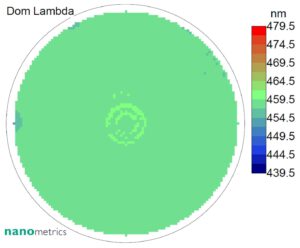
Inside the production
Industries
Processes & technical limits
| Processes | Tolerance | Max. part | Weight | Lot size | Materials |
|---|---|---|---|---|---|
| Manufacture of GaN-on-Silicon epiwafers (epitaxy wafers for MicroLEDs)Casting | – | – | – | – | GaN-on-Silicon (epiwafer) |
| Supply of epiwafers in 200 mm and 300 mm wafer diameters (fabless via contract manufacturers)Engineering | – | – | – | – | GaN-on-Silicon |
Additional services
History
- 2014
Founded in Dresden, Germany
- 2020
First company worldwide to demonstrate a 300 mm LED epiwafer