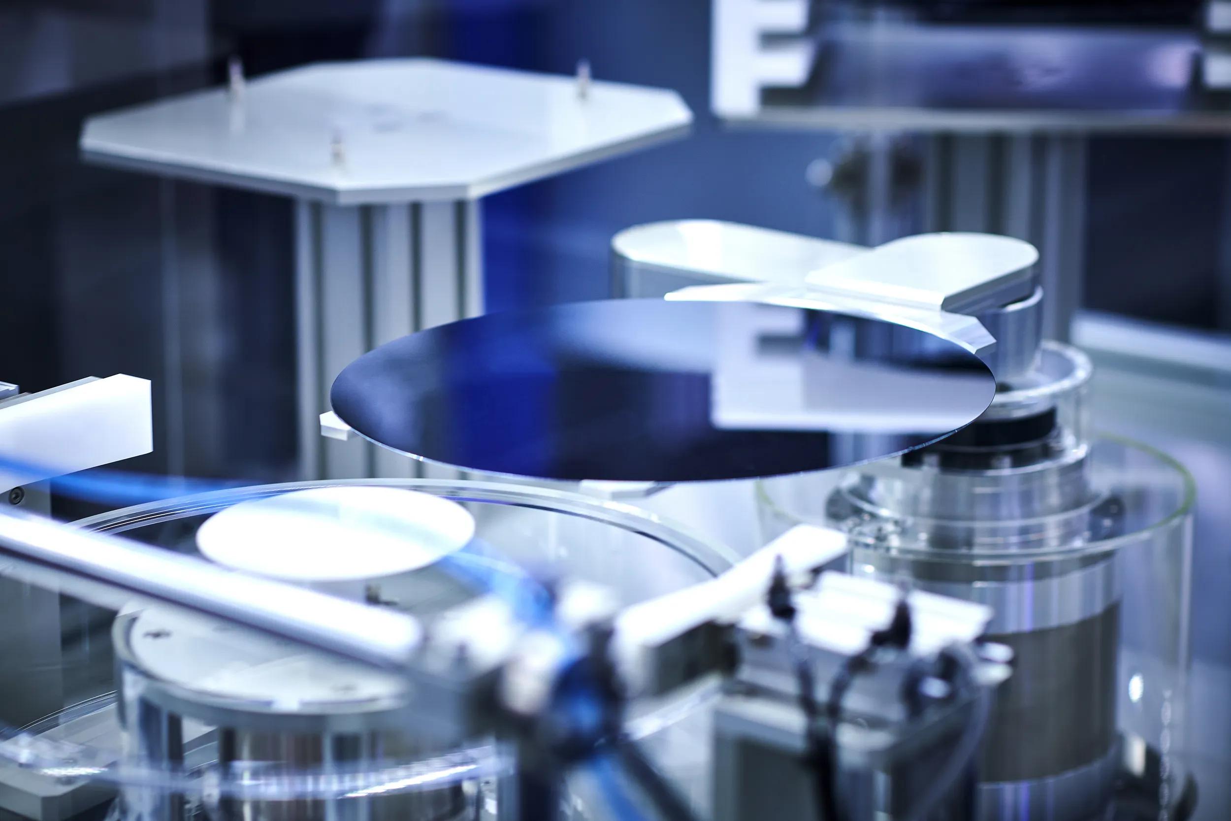
Semiconductor-based light and sensor solutions: LED chips, laser diodes, sensors and CMOS foundry services.
ams-OSRAM AG
Premstätten (AT) · Munich (DE) · Penang (MY) · Wuxi (CN) · Calamba (PH) · Singapore (SG) · Tokyo (JP) · Seoul (KR) · Taipei (TW) · Hong Kong (HK) · Beijing (CN) · Shanghai (CN) · Shenzhen (CN)New on Amplifa
About ams OSRAM
ams-OSRAM AG, headquartered in Premstätten/Graz (Austria) with a co-headquarters in Munich (Germany), is a technology company for light and sensor technology. Its portfolio comprises semiconductor-based light emitters (LEDs, laser diodes, VCSELs), optical sensors, time-of-flight sensors, CMOS ICs as well as traditional lighting technologies for automotive and specialty applications. The full-service foundry manufactures analog and mixed-signal CMOS processes (110 nm, 180 nm, 350 nm), high-voltage CMOS and BiCMOS on 200-mm wafers, complemented by wafer sort, packaging, final test and special technologies such as TSV, die stitching, trench dicing, 3D-IC integration and optical filters. The material base is silicon wafers and III-V semiconductor material systems. The manufacturing sites in Europe are automotive-certified and medical-grade, plus a wafer fab in Penang (Malaysia). Core markets are Automotive & Mobility, Industrial, Medical & Health, Consumer Electronics, Lighting, Computing as well as Aerospace. The company employs around 18,500 people and generated revenue of 3.3 billion euros in 2025.
- Site
- Premstätten, Austria
- Processes
- CMOS foundry manufacturing (analog/mixed-signal), CMOS process nodes 110nm, 180nm, 350nm; high-voltage CMOS, BICMOS, RF, low-noise, high-voltage, BCD, Through Silicon Via (TSV), electrical and optical, Die stitching (joining multiple reticles on one wafer in photolithography), Optical filters (various types), Trench dicing, 3D-IC integration, Wafer sort (wafer sorting and testing)
- Materials
- Silicon (wafer), CMOS silicon (photodiodes with vapor-deposited interference filters), Copper (for blue-laser absorption in material processing), Gold (reflective metals for blue-laser applications), III-V semiconductor material systems (LED/laser, used in automotive/industrial for decades), Silicon (200 mm wafer), III-V semiconductor material systems, Copper
- Certificates
- ISO 9001, IATF 16949, ISO 14001, ISO 45001, ISO 50001, ISO 27001, TISAX
- Founded
- 1906
- Employees
- 18500
- Industries
- Automotive & Mobility, Industrial, Medical & Health, Consumer Electronics (Mobile & Wearables), Lighting, Computing
- 01
IC design & design support (ASIC, simulation, IP)
- 02
CMOS/HV-CMOS/BiCMOS wafer fabrication on 200 mm (8-inch)
- 03
Photolithography including die stitching
- 04
Special technologies (TSV, 3D-IC, optical filters)
- 05
Post-wafer processing (sawing/trench dicing, sorting)
- 06
Wafer sort (test)
- 07
Packaging / assembly (including WLCSP, tape and reel)
- 08
Final test
- 09
Supply chain management & delivery
Materials & Processes
Silicon (200 mm wafer)
Carrier material for CMOS mixed-signal ICs, sensors and photodiodes with vapor-deposited interference filters.
III-V semiconductor material systems
Basis for LED chips (thin-film technology), laser diodes, laser bars and micro-emitter arrays.
Copper
Target material for blue-laser absorption (450 nm) in material processing.
Gold
Reflective metal for blue-laser applications.
Polymer film (ALIYOS™)
Carrier material for ultra-thin LED films (< 1 mm) in LED-on-foil technology.
Locations
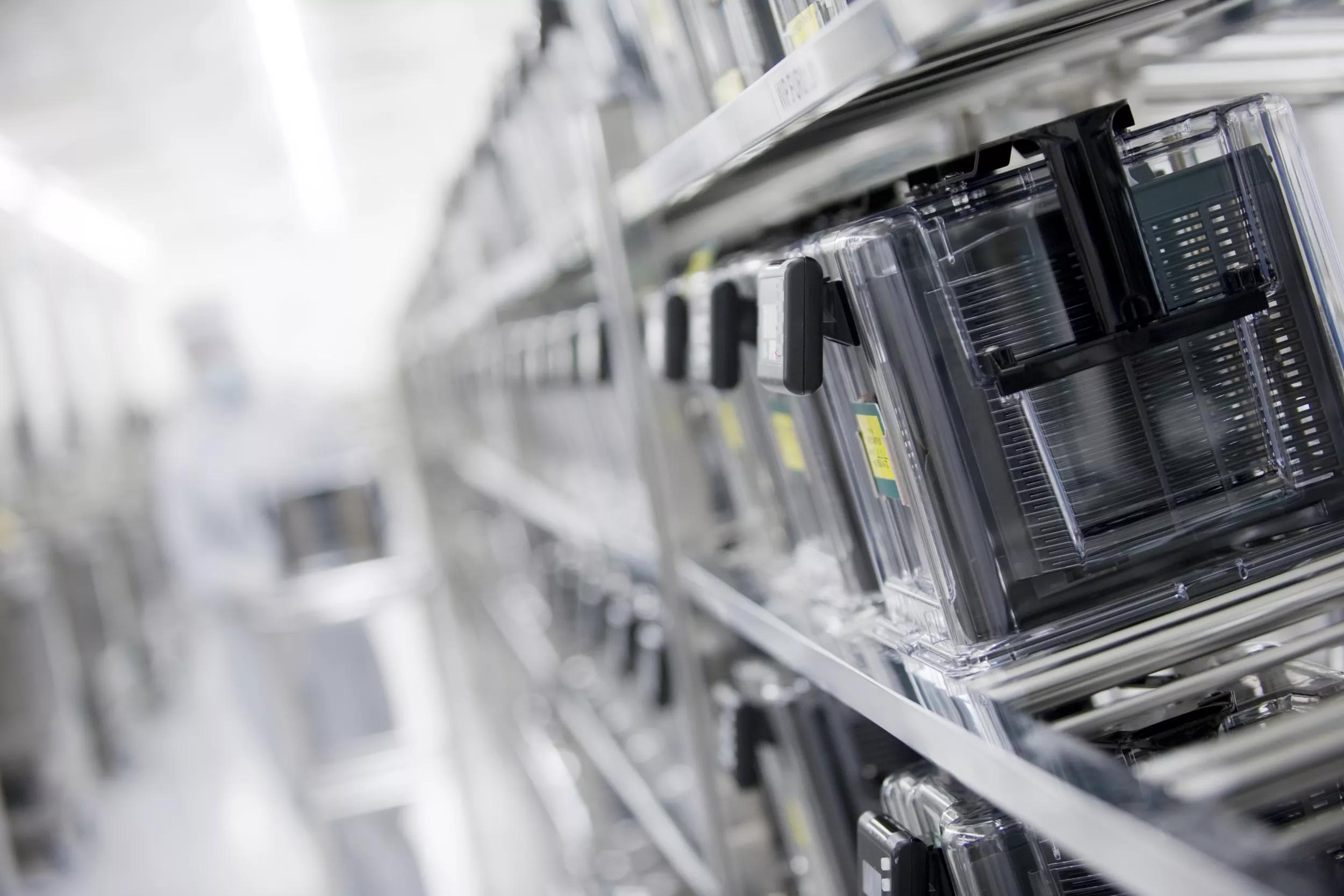
Premstätten
ATHeadquarters, semiconductor manufacturing (automotive-certified, medical grade)
- Materials
- Silicon
- 200 mm (8-inch) wafer fab
- Test and sorting equipment
- Packaging/assembly equipment
Munich
DECo-headquarters
Penang
MYManufacturing (wafers)
- Materials
- Silicon
- Wafer fab
Wuxi
CNManufacturing/branch office
Calamba
PHBranch office (ams Asia Inc.)
Foshan
CNBranch office
Components & Products
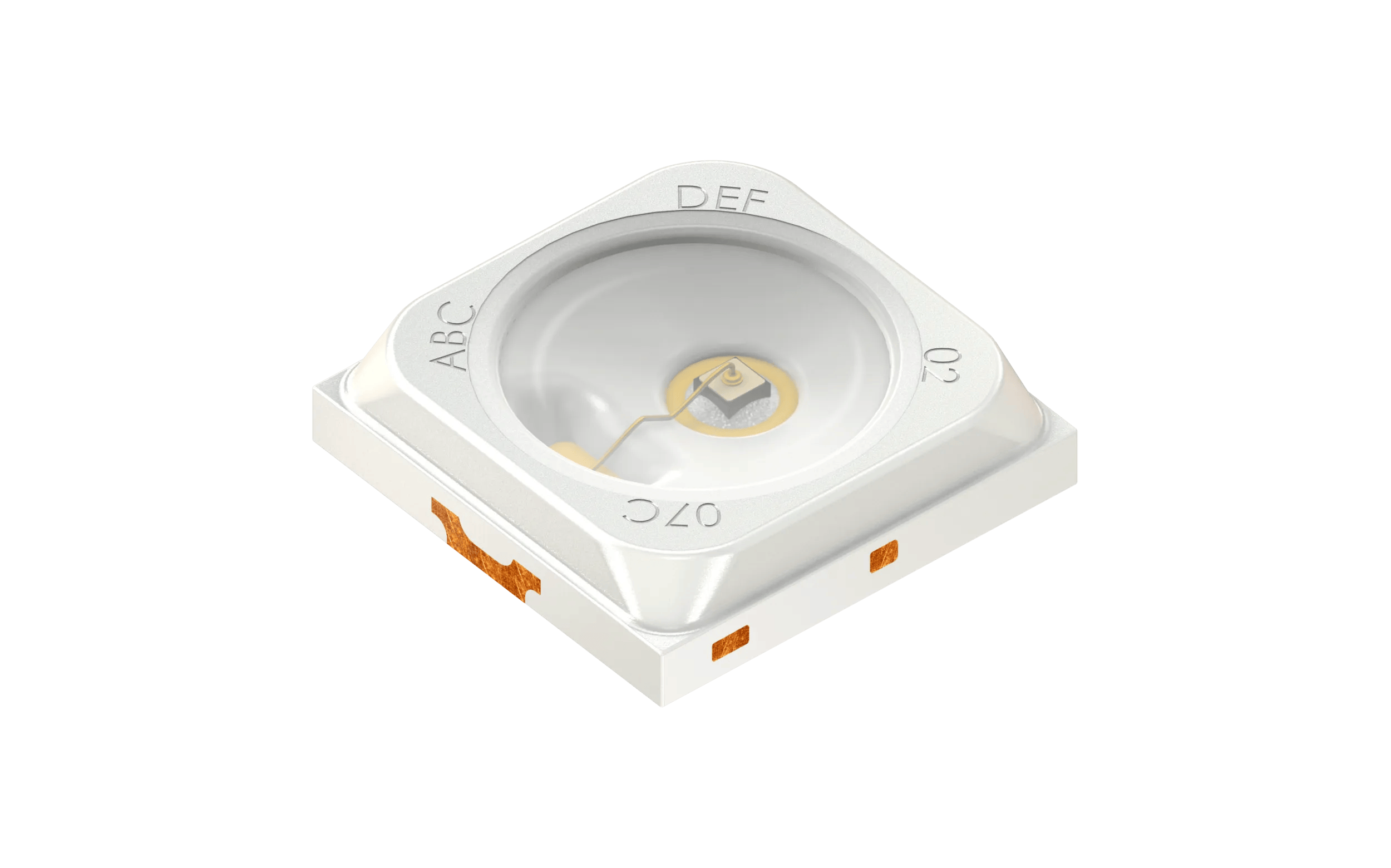
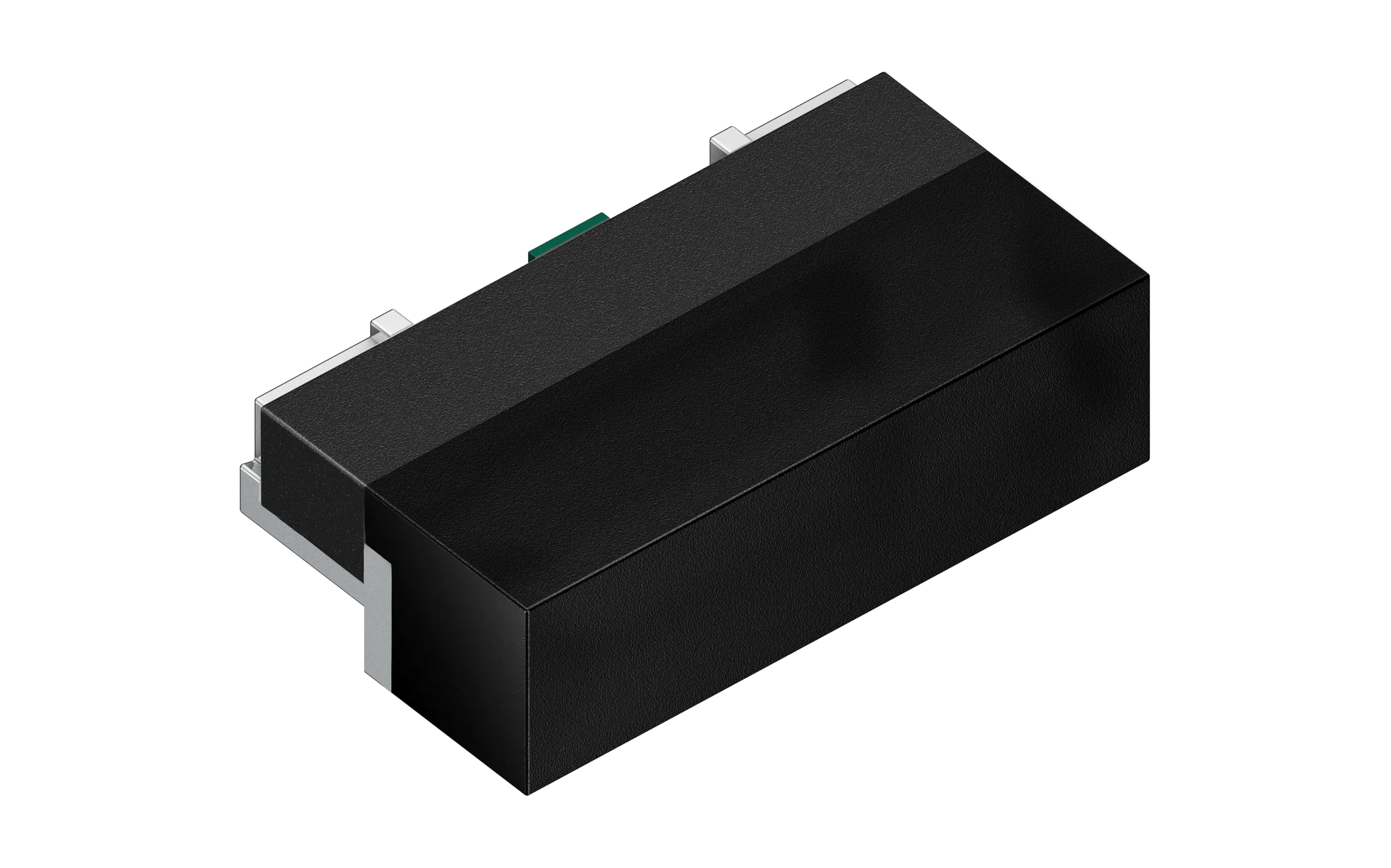
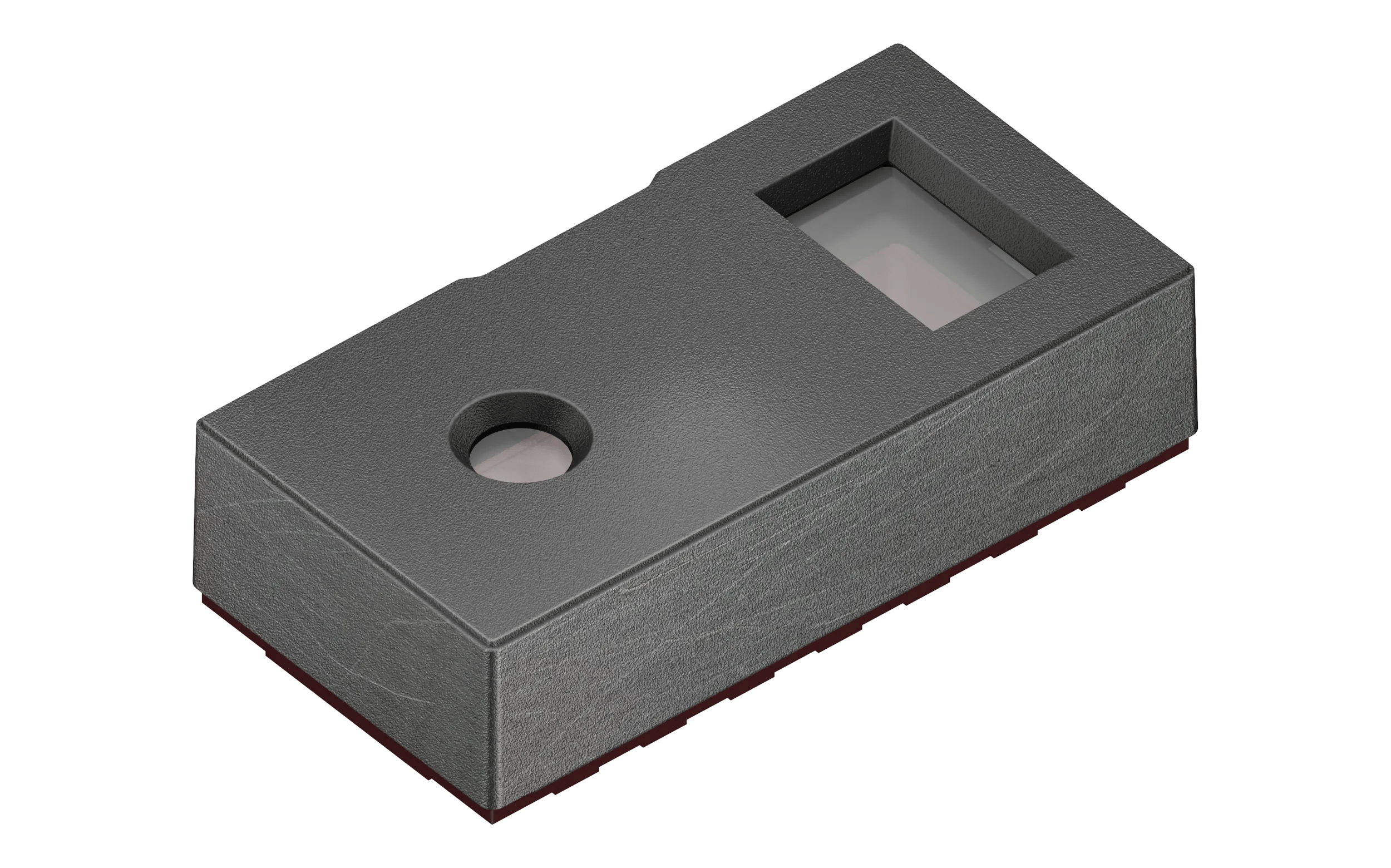
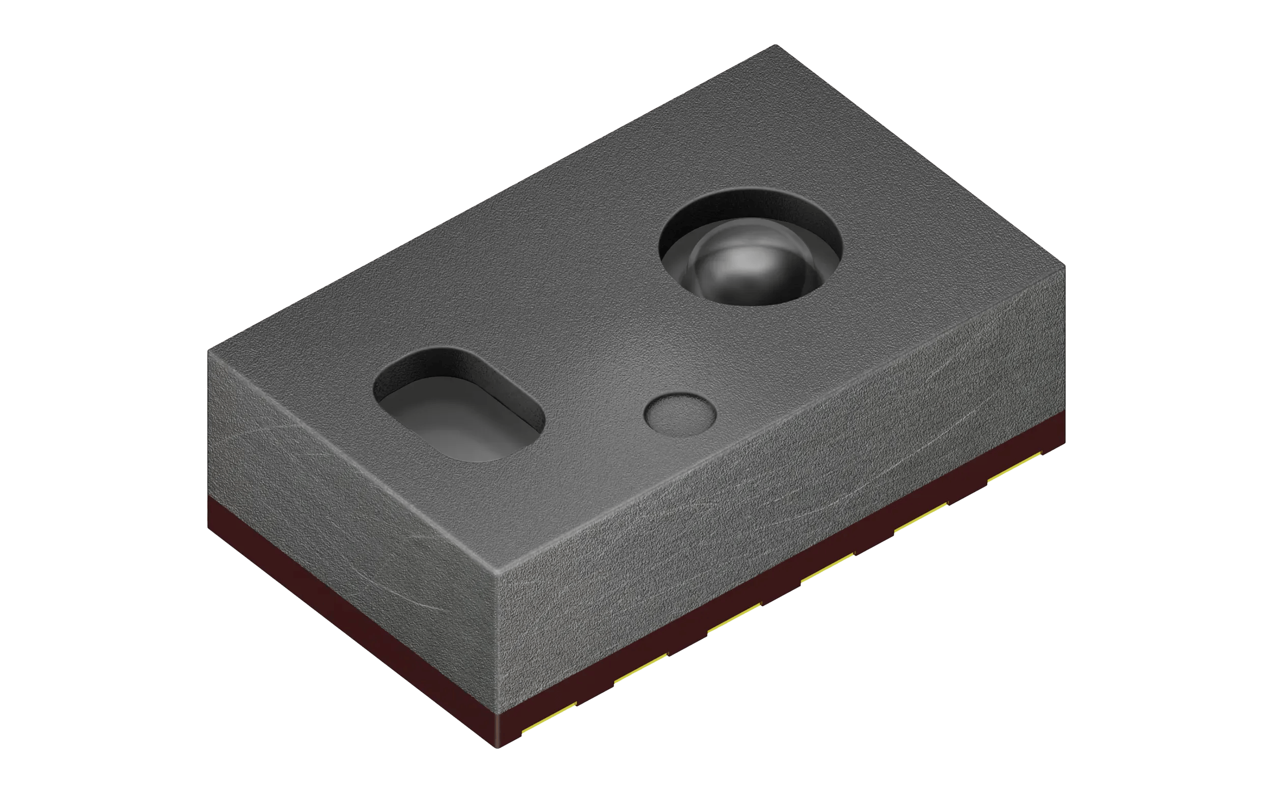
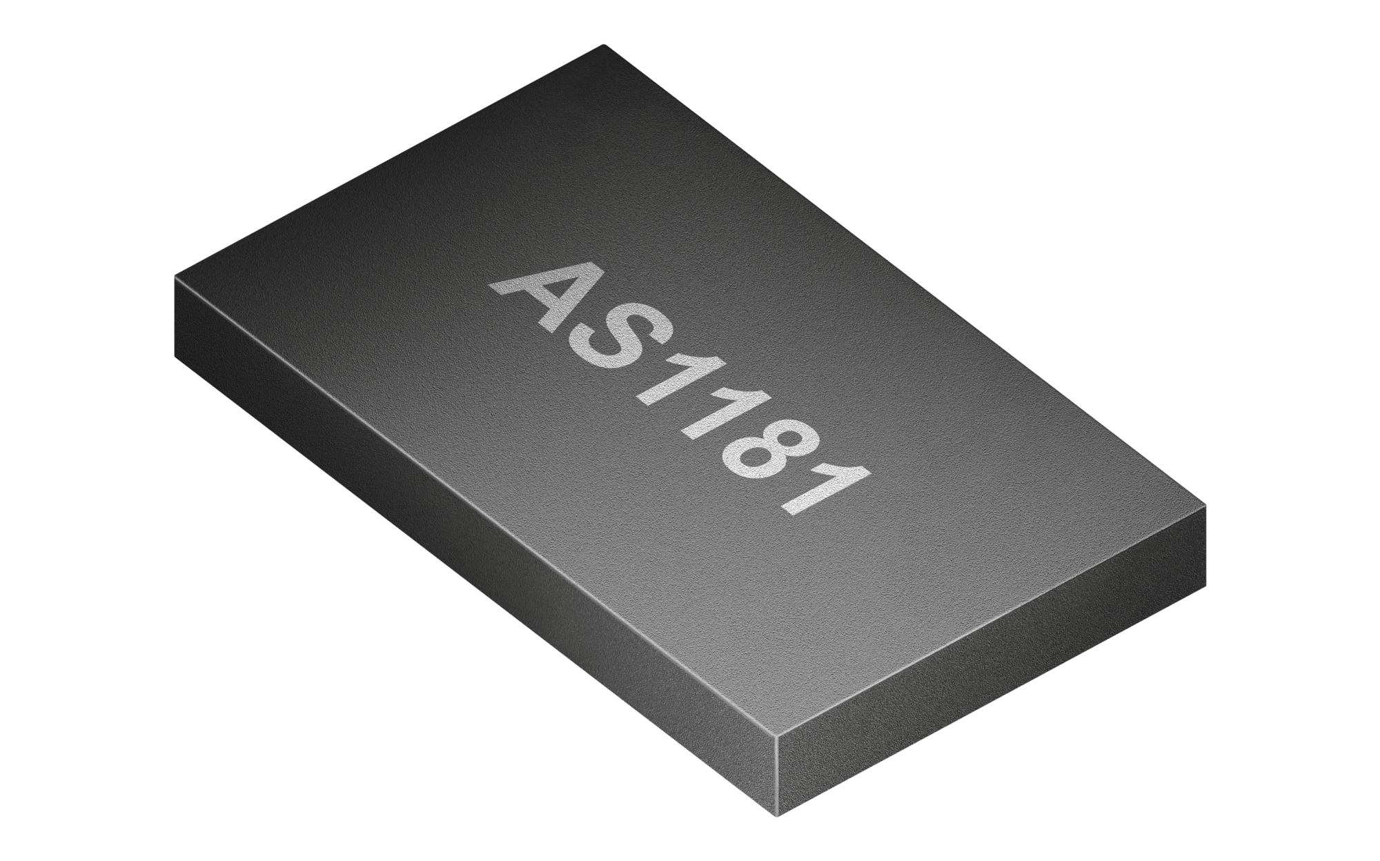
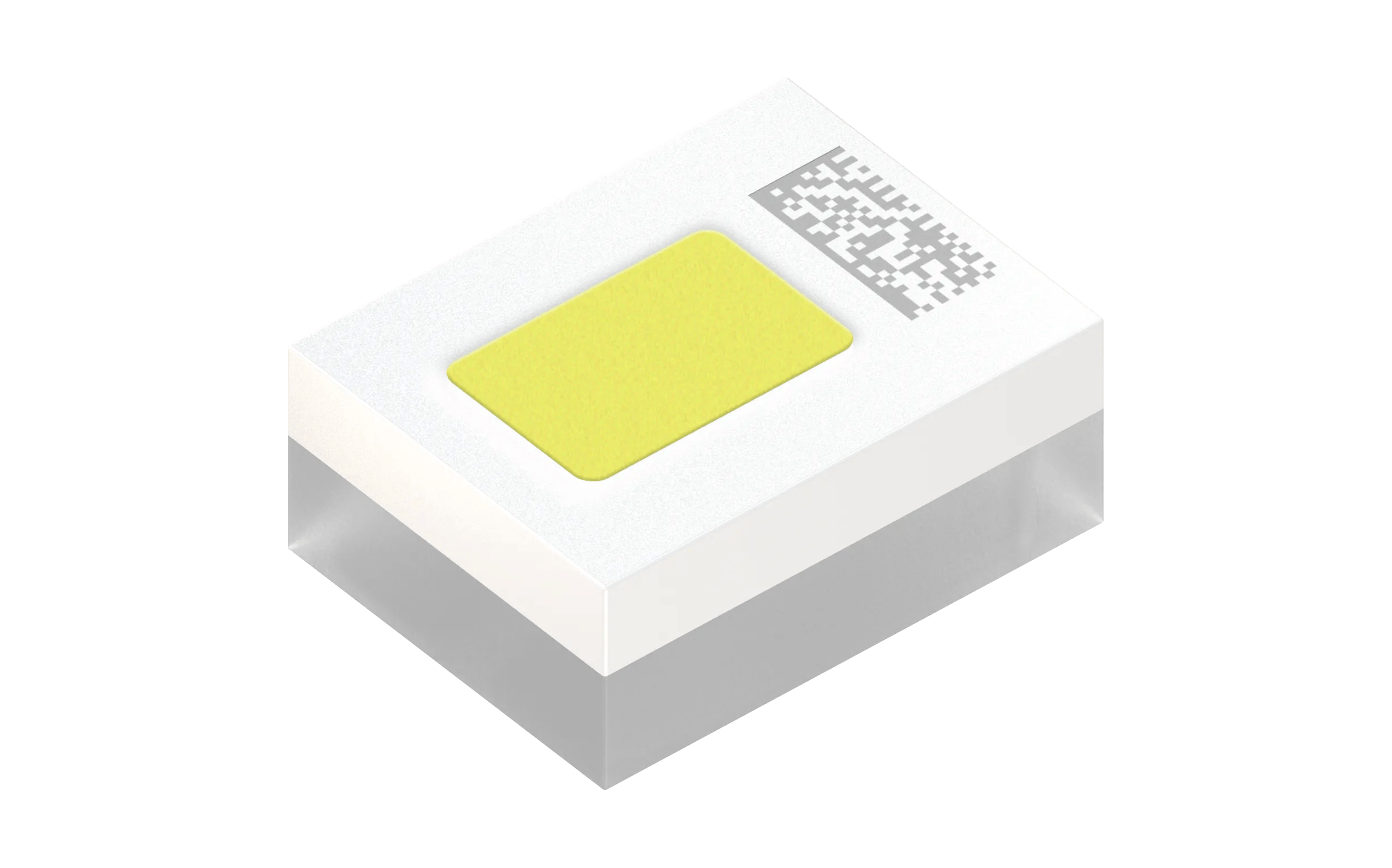
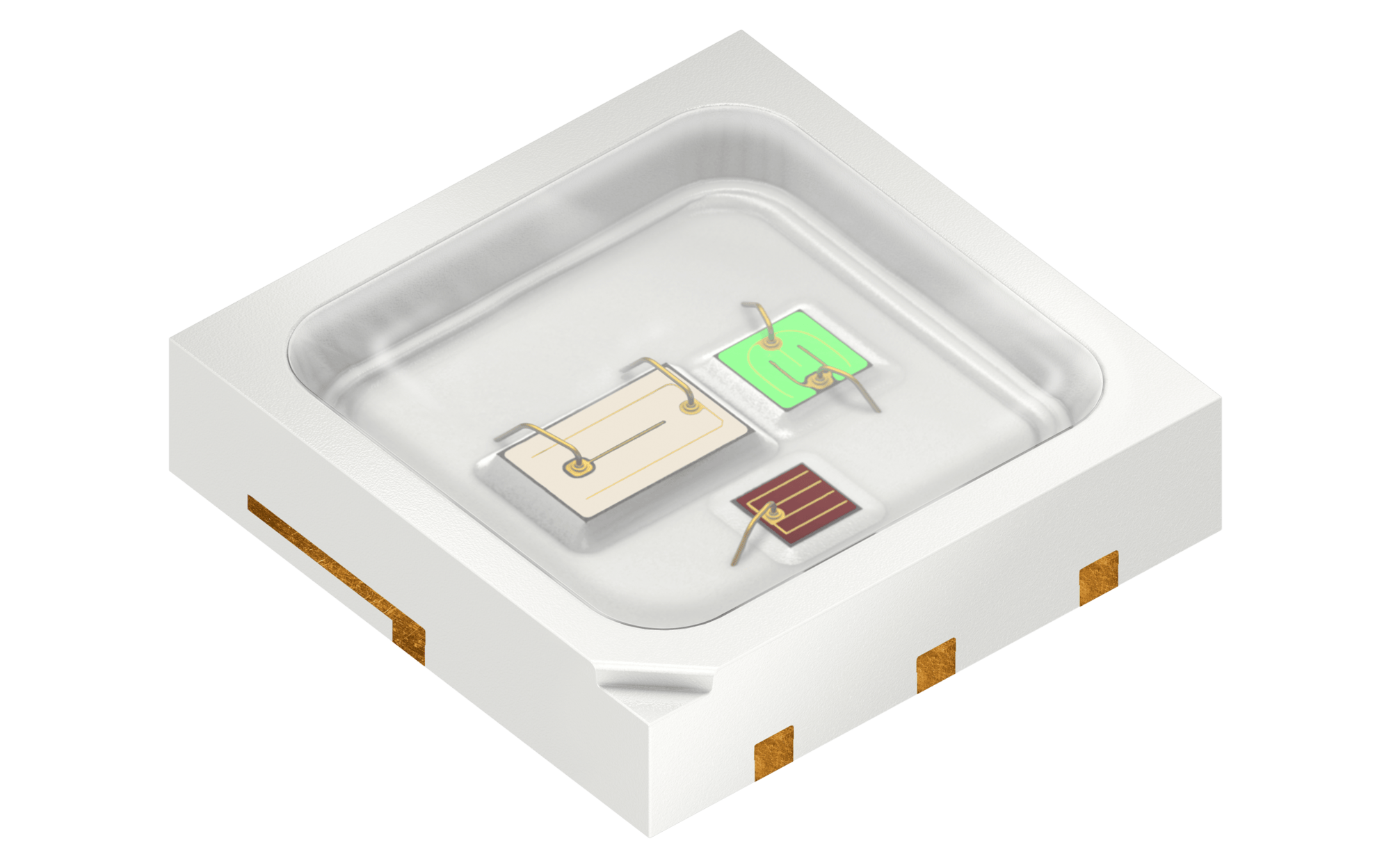
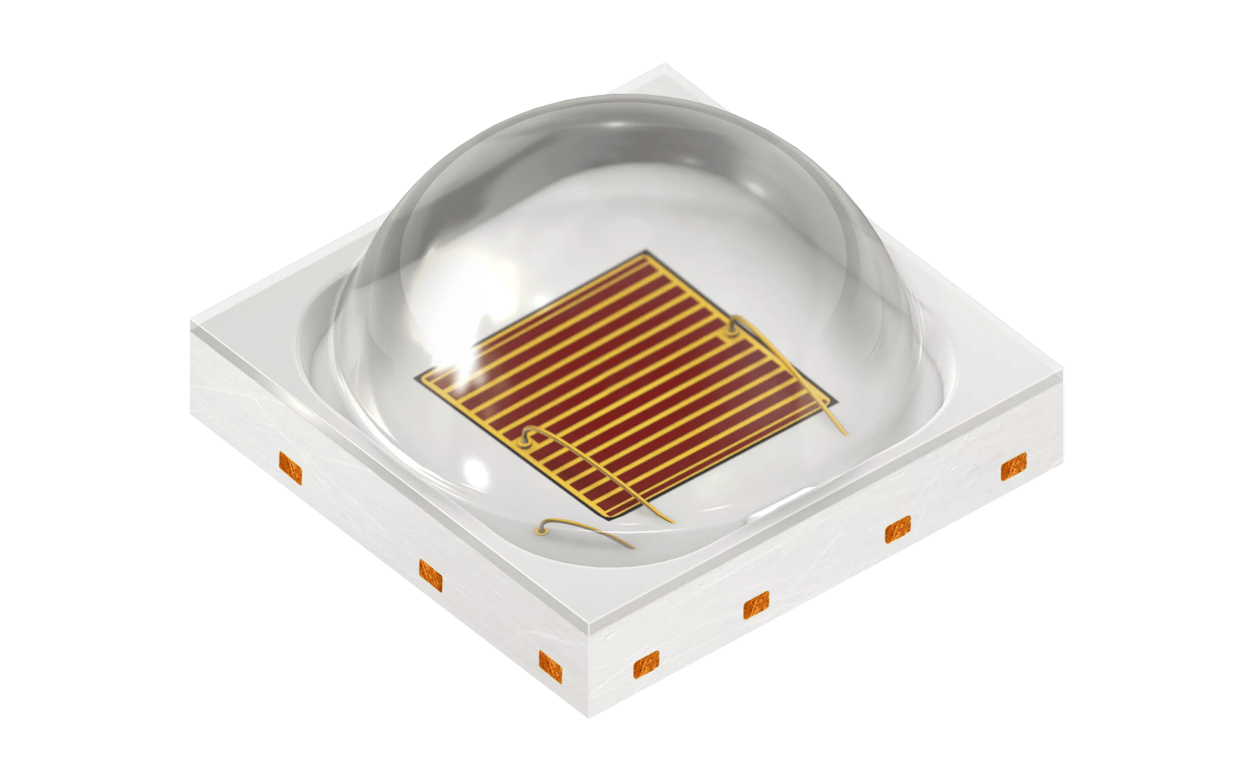
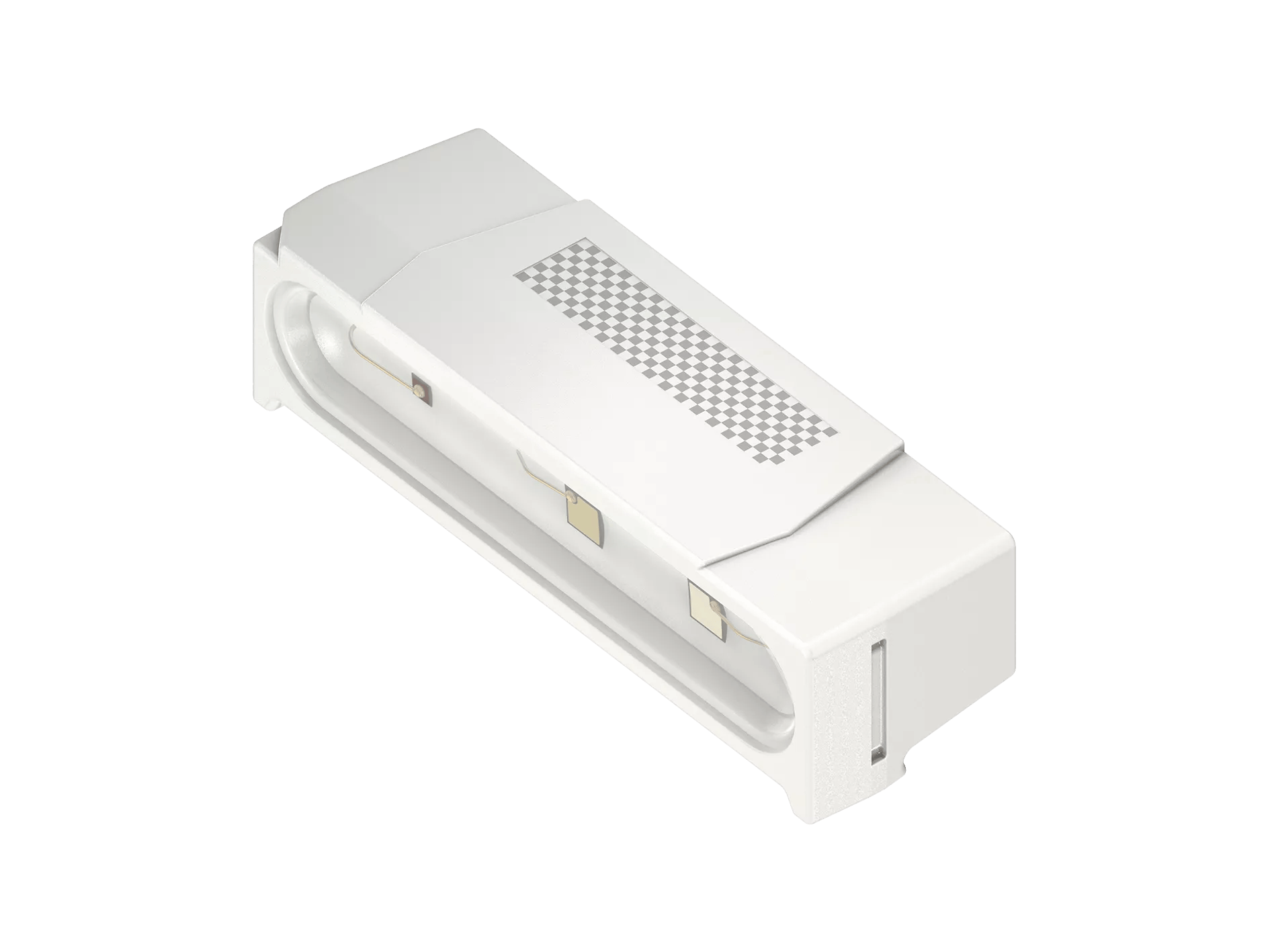
Inside the production
Industries
Processes & technical limits
| Processes | Tolerance | Max. part | Weight | Lot size | Materials |
|---|---|---|---|---|---|
| CMOS foundry manufacturing (analog/mixed-signal)Engineering | – | – | – | – | Silicon (200mm/8-inch wafers) |
| CMOS process nodes 110nm, 180nm, 350nm; high-voltage CMOS, BICMOS, RF, low-noise, high-voltage, BCDEngineering | – | – | – | – | Silicon |
| Through Silicon Via (TSV), electrical and opticalJoining | – | – | – | – | Silicon |
| Die stitching (joining multiple reticles on one wafer in photolithography)Joining | – | – | – | – | Silicon |
| Optical filters (various types)Surface | – | – | – | – | – |
| Trench dicingMachining | – | – | – | – | Silicon |
| 3D-IC integrationJoining | – | – | – | – | Silicon |
| Wafer sort (wafer sorting and testing)Testing | – | – | – | – | Silicon |
| Final test of ICs (mixed-signal)Testing | – | – | – | – | Silicon |
| Packaging / assembly (e.g. tape and reel, WLCSP)Joining | – | – | – | – | Silicon |
| Post-wafer processing: sawing, sorting, packagingMachining | – | – | – | – | Silicon |
| Manufacture of LED chips (thin-film technology, Thinfilm IR:6 chip technology)Additive | – | – | – | – | Semiconductor (III-V), silicon |
| Manufacture of laser diodes and laser bars (e.g. 5-junction edge-emitting laser, blue laser 450 nm)Additive | – | – | – | – | Semiconductor (III-V) |
| Micro-emitter arrays / 2D arrays for optical interconnects (EVIYOS)Additive | – | – | – | – | Semiconductor (III-V) |
| LED-on-foil technology ALIYOS™ (ultra-thin LED films <1 mm)Joining | – | – | – | – | Film/plastic |
| ASIC development and manufacturingEngineering | – | – | – | – | Silicon |
| Semiconductor manufacturing sites with automotive-certified and medical-grade facilitiesEngineering | – | – | – | – | Silicon |
3 Anlagen & Maschinen
| Machine | Manufacturer / model | Quantity | Working area | Year built | Site |
|---|---|---|---|---|---|
| Semiconductor manufacturing equipment (wafer fab, 200 mm / 8-inch) | – | – | – | – | Europe (automotive-certified, medical grade) |
| Test and sorting equipment (wafer sort, final test) | – | – | – | – | – |
| Packaging/assembly equipment | – | – | – | – | – |
Additional services
Reference customers
Quality & Certifications
The manufacturing sites in Europe are automotive-certified and meet medical-grade requirements; quality management includes wafer sort, final test and precise characterization with advanced design tools.
| Evidence | Premstätten |
|---|---|
| ISO 9001 | |
| IATF 16949 | |
| ISO 14001 | |
| ISO 45001 | |
| ISO 50001 | |
| ISO 27001 | |
| TISAX |
History
- 1906
OSRAM registered as a brand
- 1919
Merger of lamp production under OSRAM
- 1925
BILUX® dual-filament lamp
- 1936
first fluorescent lamp
- 1954
Xenon short-arc lamp
- 1967
Halogen lamp
- 1976
first infrared LEDs
- 1996
first white-converted LED
- 2001
Thin-film technology
- 2021
Launch of ams OSRAM
- 2023
Volume shipments of EVIYOS to the automotive industry
- 2024
German Future Prize for 'Digital Light'
- 2025
Revenue €3.3 billion
- 2026
120 years of the OSRAM brand