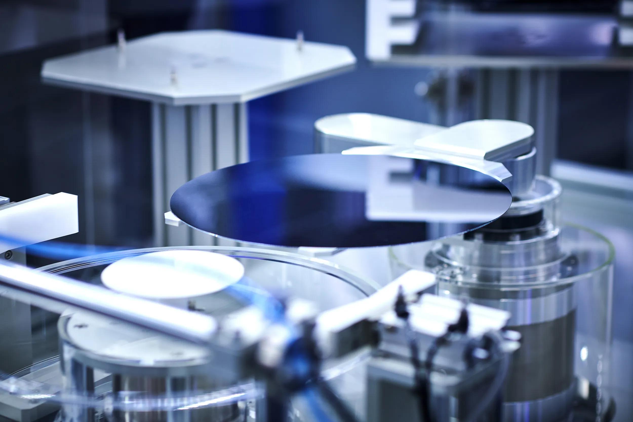
Develops and manufactures semiconductor-based light and sensor solutions as well as CMOS ICs as a full-service foundry.
ams-OSRAM AG
Premstätten (AT) · Munich (DE) · Penang (MY) · Wuxi (CN) · Calamba City (PH) · Foshan (CN) · Tokyo (JP) · Seoul (KR) · Singapore (SG) · Taipei (TW) · Hong Kong (HK) · Gurgaon (IN) · Dubai (AE) ·New on Amplifa
About ams OSRAM
ams OSRAM is a globally operating technology company for light and sensor technology with headquarters in Premstätten (Austria) and a co-headquarters in Munich. The company develops and manufactures semiconductor-based light emitters (LEDs, laser diodes, VCSELs), optical sensors and CMOS integrated circuits for applications in automotive, industrial, medical and consumer electronics. As a full-service foundry, ams OSRAM additionally offers the manufacturing of mixed-signal ICs on 200-mm silicon wafers in CMOS processes (110, 180 and 350 nm) as well as high-voltage CMOS and BiCMOS, complemented by wafer sort, packaging, final test, TSV, die stitching, optical filters and 3D IC integration. The manufacturing sites include, among others, Premstätten, Penang (Malaysia) and Wuxi (China). With around 18,500 employees and revenue of 3.3 billion euros (2025) as well as around 12,000 patents and patent applications, the company sets standards in digital photonics. The OSRAM brand has existed since 1906 and has been part of ams OSRAM since 2021.
- Site
- A-8141 Premstätten
- Processes
- CMOS / mixed-signal foundry (110nm, 180nm, 350nm), High-voltage CMOS, BiCMOS, Specialty processes: RF, low-noise, high-voltage, BCD, Through Silicon Vias (TSV), electrical and optical, Die stitching (reticle merging in photolithography), Optical filters (integrated on-chip), Trench dicing
- Materials
- Silicon (CMOS wafers), Copper, Gold
- Certificates
- ISO 9001, IATF 16949, ISO 14001, ISO 45001, ISO 50001, ISO 27001, TISAX
- Founded
- 1906
- Employees
- 18500
- Industries
- Automotive & Mobility, Industrial, Medical & Health, Mobile & Wearables, Lighting, Computing
- 01
IC design support and IP consulting
- 02
Wafer fabrication (CMOS/BiCMOS, 200 mm)
- 03
Wafer sort / testing
- 04
Sawing (trench dicing) and sorting
- 05
Assembly / packaging (TSV, die stitching, optical filters)
- 06
Final test (tape and reel)
- 07
Supply chain management and second source
Materials & Processes
Silicon (CMOS wafers)
Base material of the foundry processes (CMOS, HV-CMOS, BiCMOS, BCD) on 200-mm wafers.
Copper
Target material for blue 450-nm laser diodes in material processing of reflective metals.
Gold
Machinable with 450-nm blue lasers for applications such as battery welding.
Locations
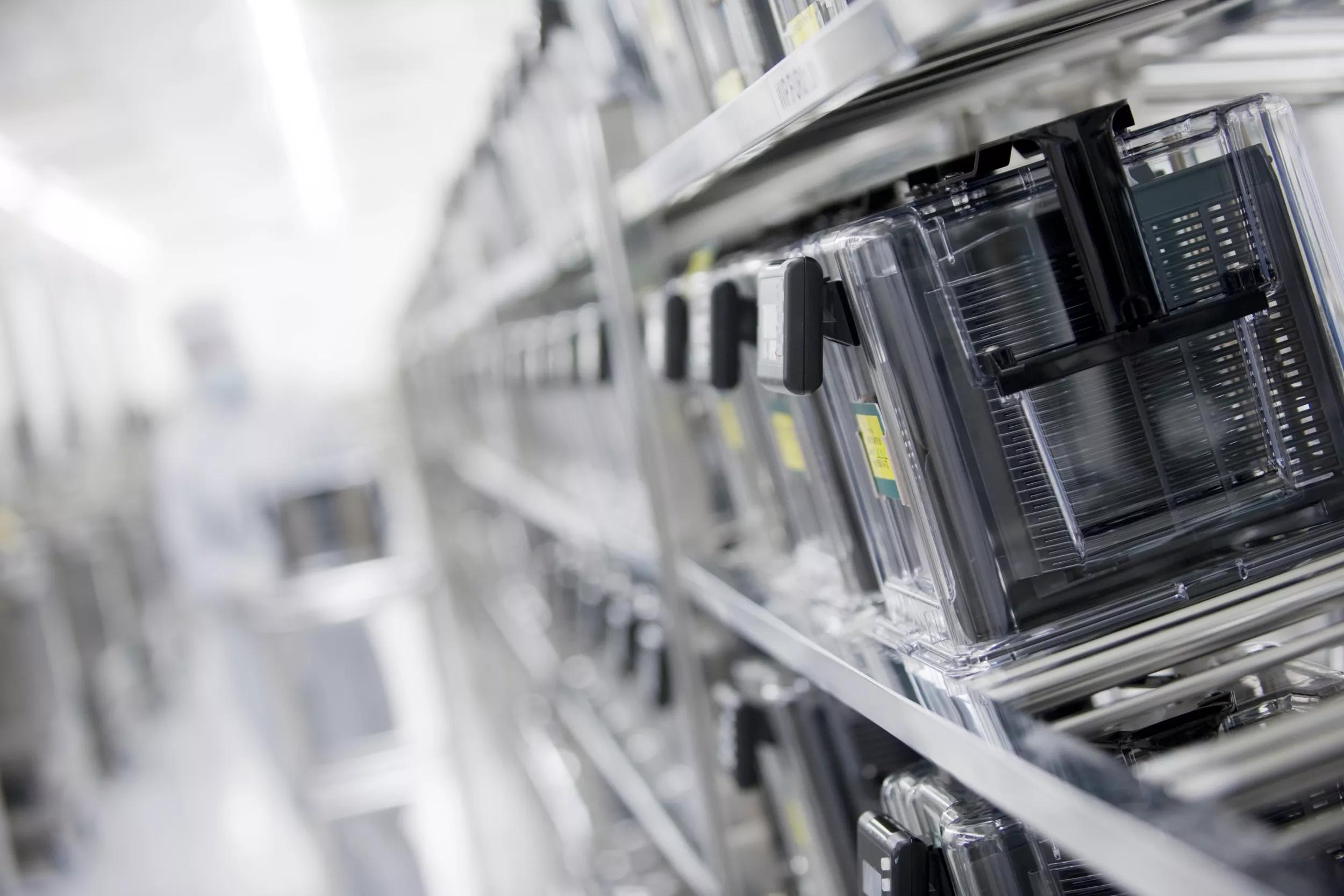
Premstätten
ATHeadquarters, manufacturing and development
- Materials
- Silicon
- 200-mm wafer fab
Munich
DECo-headquarters
Penang
MYManufacturing (OSRAM Opto Semiconductors)
Wuxi
CNManufacturing (OSRAM Opto Semiconductors China)
Calamba City
PHSite (ams Asia Inc.)
Products & Components
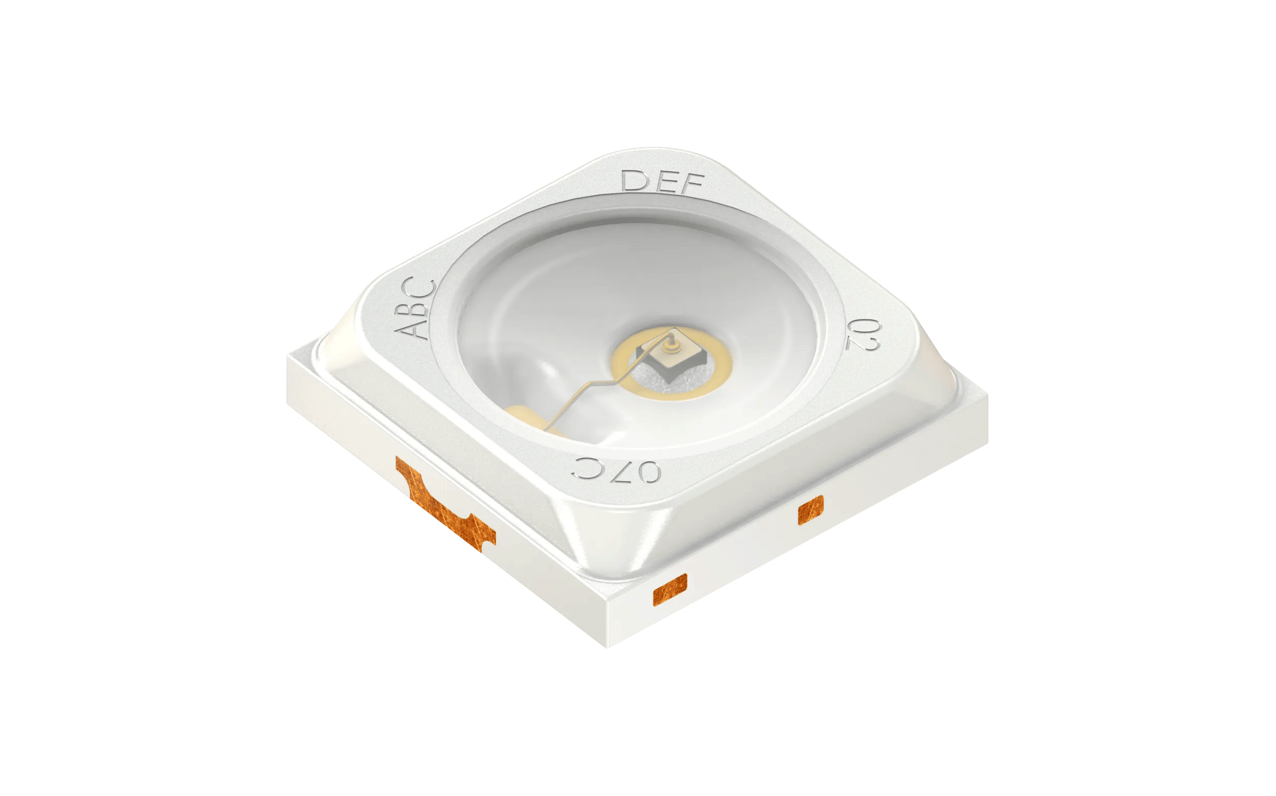
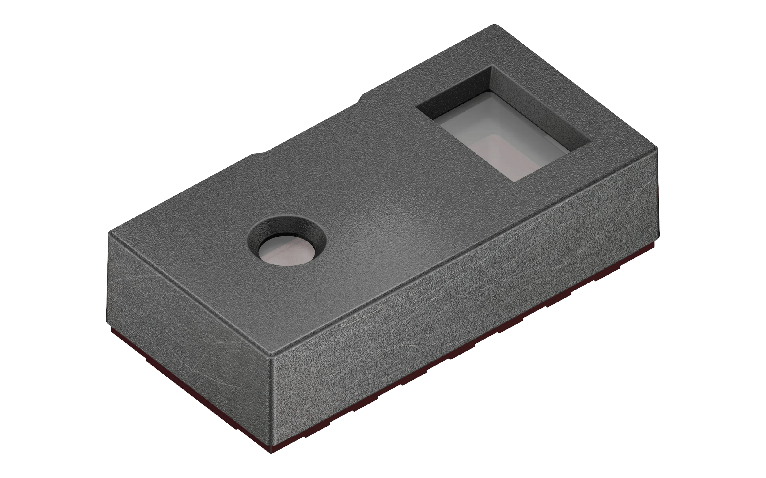
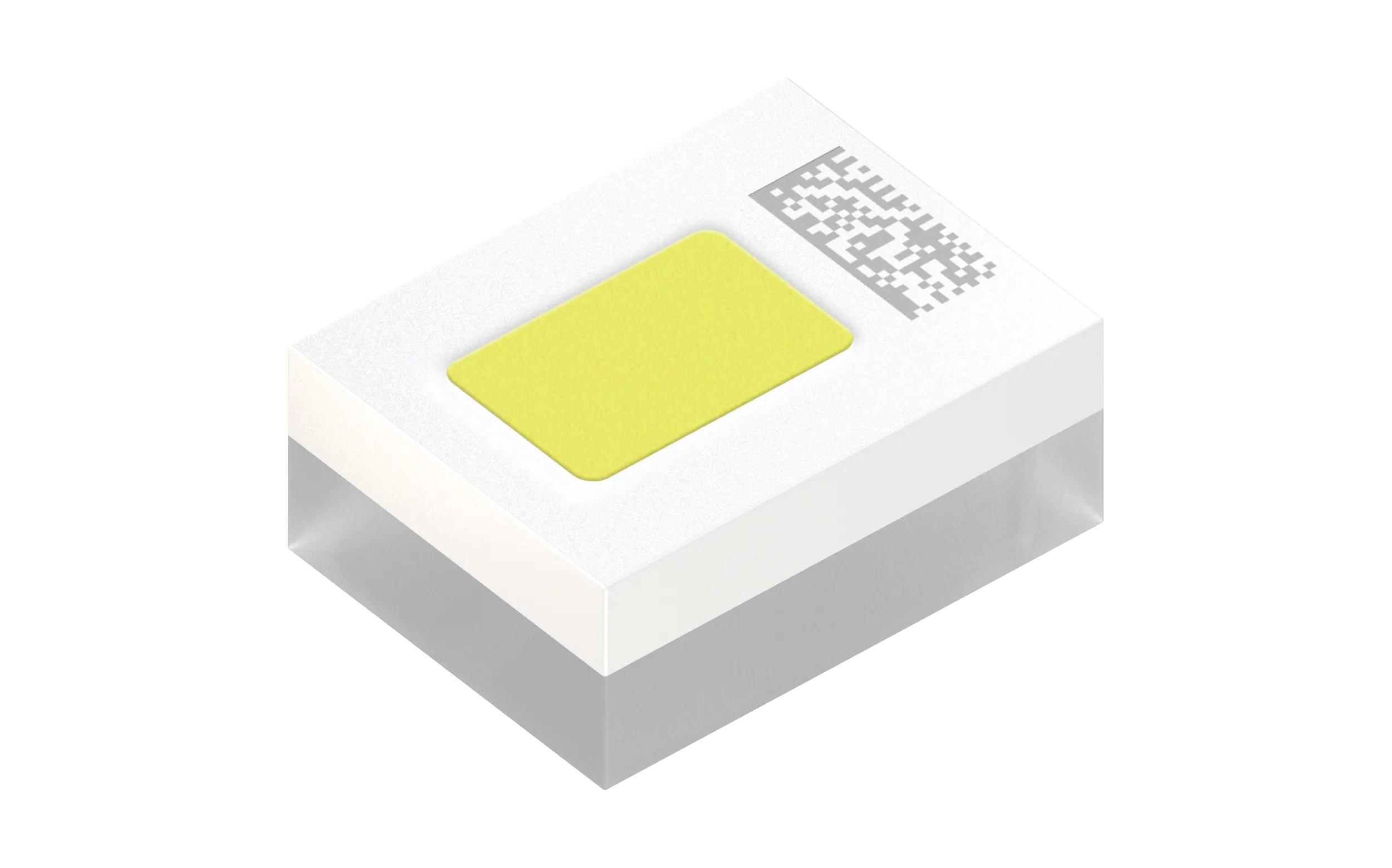
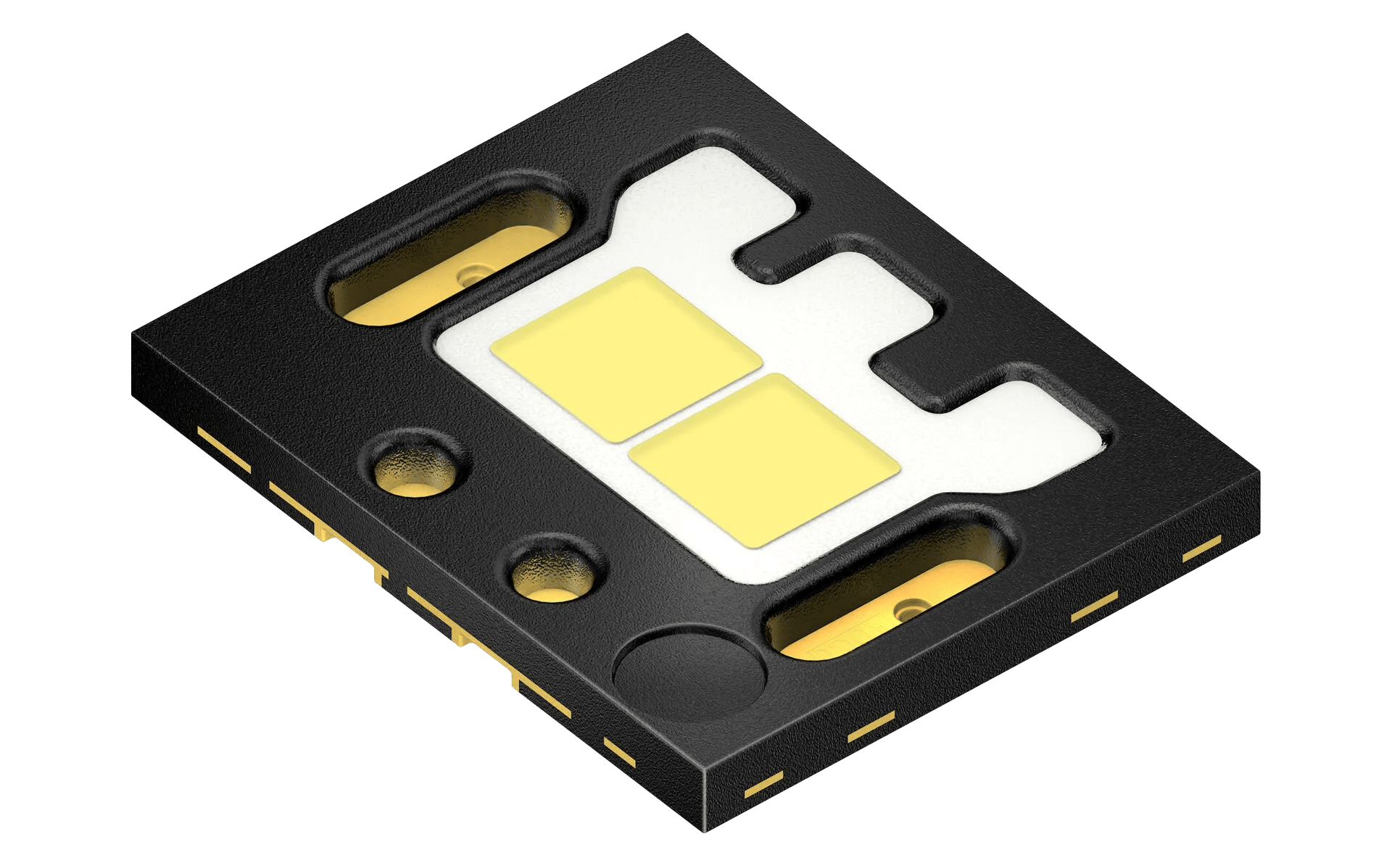
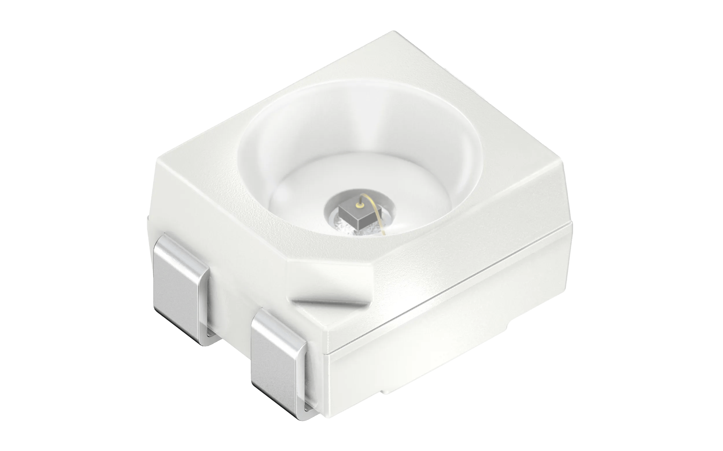
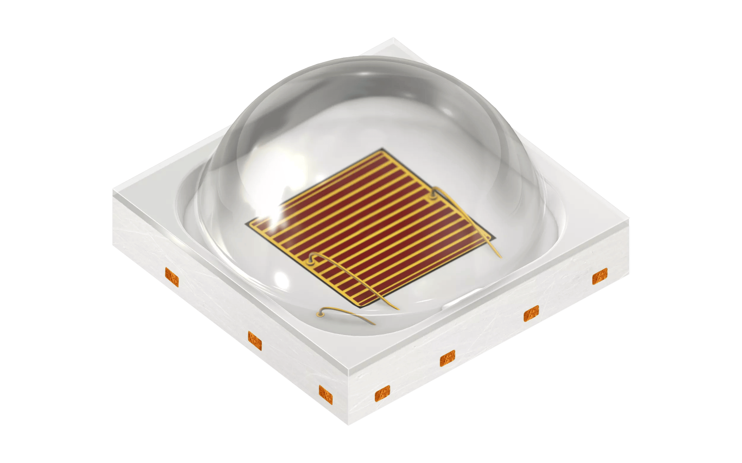
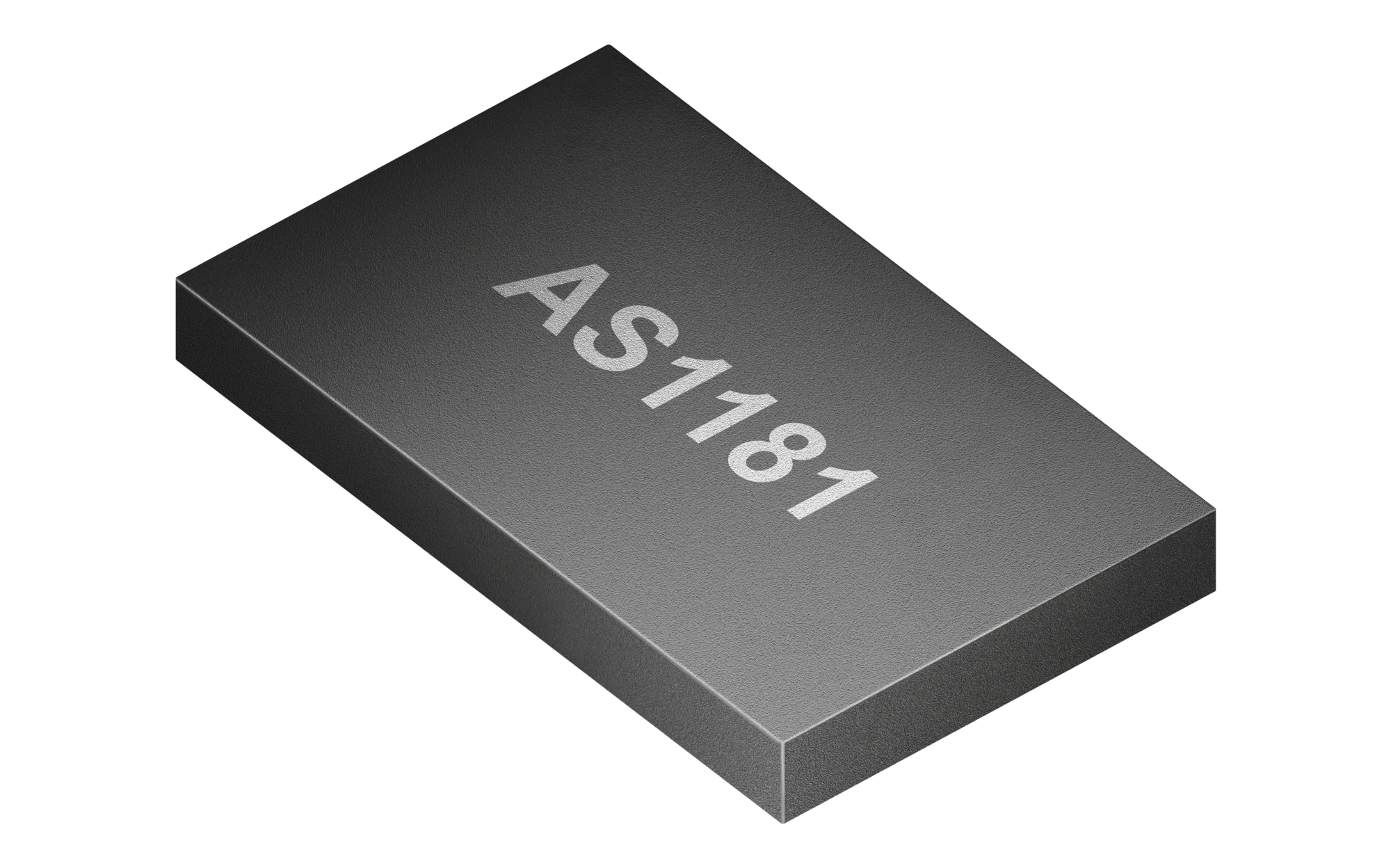
Inside the production


Industries
Processes & technical limits
| Processes | Tolerance | Max. part | Weight | Lot size | Materials |
|---|---|---|---|---|---|
| CMOS / mixed-signal foundry (110nm, 180nm, 350nm)Semiconductor manufacturing | – | 200 mm (8-inch wafer) | – | – | Silicon |
| High-voltage CMOSSemiconductor manufacturing | – | – | – | – | Silicon |
| BiCMOSSemiconductor manufacturing | – | – | – | – | Silicon |
| Specialty processes: RF, low-noise, high-voltage, BCDSemiconductor manufacturing | – | – | – | – | Silicon |
| Through Silicon Vias (TSV), electrical and opticalSemiconductor manufacturing | – | – | – | – | Silicon |
| Die stitching (reticle merging in photolithography)Semiconductor manufacturing | – | – | – | – | Silicon |
| Optical filters (integrated on-chip)Semiconductor manufacturing | – | – | – | – | – |
| Trench dicingSemiconductor manufacturing | – | – | – | – | Silicon |
| 3D IC integrationSemiconductor manufacturing | – | – | – | – | Silicon |
| Wafer sort / testingTesting | – | – | – | – | Silicon |
| Assembly / packaging / final test (tape and reel)Assembly | – | – | – | – | Silicon |
| Sawing and sorting of wafers/diesSemiconductor manufacturing | – | – | – | – | Silicon |
| Thin-film VCSEL / edge-emitting laser (5-junction)Semiconductor manufacturing | – | – | – | – | – |
| LED chip manufacturing (Thinfilm IR:6 chip technology)Semiconductor manufacturing | – | – | – | – | – |
| Micro-emitter arrays / 2D micro-array technology for optical interconnectsSemiconductor manufacturing | – | – | – | – | – |
| ALIYOS LED-on-foil technology (foil manufacturing, < 1 mm stack height)Semiconductor manufacturing | – | < 1 mm | – | – | – |
| High-power laser bars/diodes for material processing (808–1020 nm, up to 500 W; blue 450 nm lasers)Semiconductor manufacturing | – | – | – | – | Copper, Gold |
Additional services
Reference customers
Quality & Certifications
Manufacturing is automotive-certified and medical grade; quality is ensured through wafer sort, final test and characterized process windows.
| Evidence | Premstätten |
|---|---|
| ISO 9001 | |
| IATF 16949 | |
| ISO 14001 | |
| ISO 45001 | |
| ISO 50001 | |
| ISO 27001 | |
| TISAX |
History of the OSRAM Brand
- 1906
Registration of the OSRAM brand as a wordmark
- 1919
Merger of several lamp manufacturers under the OSRAM brand
- 1925
BILUX® lamp with low beam and high beam
- 1936
Introduction of the first fluorescent lamp
- 1954
Xenon short-arc lamp for cinema, stage and TV (Oscar awards 1983 and 1987)
- 1967
Introduction of the halogen lamp
- 1974
Colored LEDs for automotive instrument panels
- 1976
First infrared LEDs
- 1996
First white-converted LED
- 2001
Introduction of thin-film technology for LED chips
- 2021
Launch of ams OSRAM – the OSRAM brand becomes part of ams OSRAM
- 2023
Series delivery of EVIYOS products to the automotive industry
- 2024
German Future Prize for "Digital Light"
- 2026
120 years of the OSRAM brand