Development and hybridization of optoelectronic InGaAs and silicon image sensors for scientific applications

ANDANTA GmbH Detektortechnologie
OlchingNew on Amplifa
About Andanta
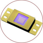
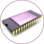
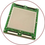
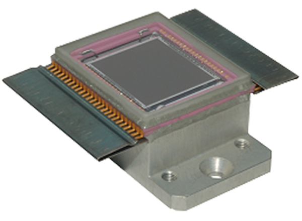
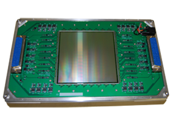
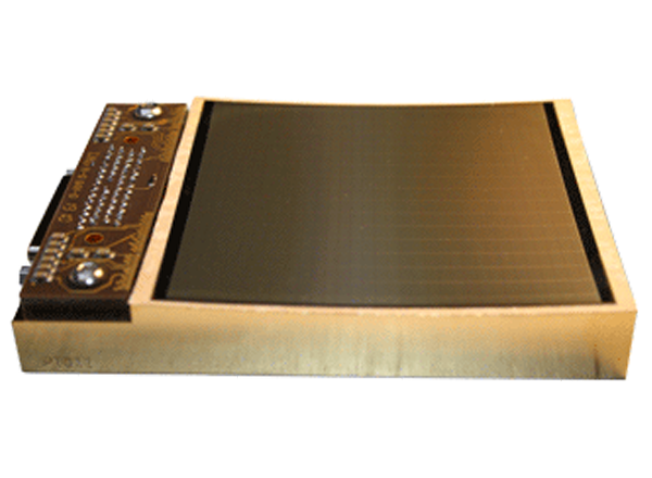
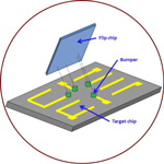
ANDANTA GmbH was founded in January 2009 and specializes in the development and provision of optoelectronic image sensors and detector arrays. The product range includes InGaAs array detectors (FPAs) and linear detectors (LDAs) for the near-infrared range (0.9–2.2 µm), high-resolution Si CCD sensors for UV to near-infrared, custom Si TDI sensors, X-ray CCDs, and curved image sensors. In addition to standard products, an increasing number of custom special developments are being created in close collaboration with manufacturing partners. The company also offers a flip-chip bonding service for the hybridization of photodiode arrays with Si-CMOS readout circuits as well as an image sensor test laboratory. Customers include camera developers and manufacturers as well as manufacturers of spectrometers, telescopes, and scientific optoelectronic systems. The company is headquartered in Olching near Munich.
- Site
- Olching
- Processes
- Flip-Chip Bonding Service (hybridization of photodiode array with Si-CMOS readout circuit), Si-CMOS readout circuit assembly / image sensor assembly, Flip-Chip Bonding Service, Image Sensor Test Laboratory, Consulting on detector solutions, Application-specific custom developments with manufacturing partners
- Materials
- Indium Gallium Arsenide (InGaAs), Silicon, Kovar, Indium Gallium Arsenide
- Certificates
- Image Sensor Test Laboratory
- Founded
- 2009
- Industries
- Camera development and manufacturing, Spectrometers, Telescopes, Scientific optoelectronic systems, NIR spectroscopy, Interferometry
- 01
Consulting on detector solutions
- 02
Custom development with manufacturing partners
- 03
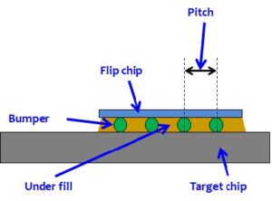
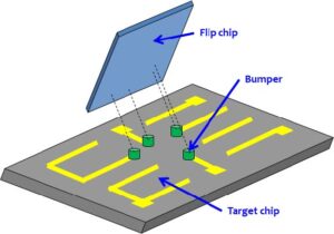
Flip-chip bonding (hybridization)
- 04
Sensor assembly
- 05
Testing in the image sensor test laboratory
- 06
Sales
Materials and Semiconductor Technologies
Indium Gallium Arsenide
Semiconductor material for NIR image sensors in the spectral range 0.9 (0.6) µm to 1.7 (2.2) µm.
Silicon
Material for CCD, CMOS and TDI image sensors for UV to near infrared (300–1100 nm).
Kovar
Package material for cooled InGaAs array and linear sensors.
Site
Olching
DEHeadquarters
- Materials
- InGaAs, silicon, Kovar
- Image sensor test laboratory
Products and Devices
Inside the production

Industries
Processes & technical limits
| Processes | Tolerance | Max. part | Weight | Lot size | Materials |
|---|---|---|---|---|---|
| Flip-Chip Bonding Service (hybridization of photodiode array with Si-CMOS readout circuit)Assembly | – | 60 mm (flip chip) / 150 mm (target chip) | – | – | InGaAs, silicon (Si-CMOS) |
| Si-CMOS readout circuit assembly / image sensor assemblyAssembly | – | – | – | – | silicon |
Additional services
Quality and Testing
An in-house image sensor test laboratory is available for the characterization and testing of the sensor assemblies; hybridization is carried out using the flip-chip process without wire bonds.
| Evidence | Olching |
|---|---|
| Image Sensor Test Laboratory |
Company History
- 2009
Foundation of ANDANTA GmbH in January; specialization in the development and provision of high-quality optoelectronic image sensors and detector arrays.
- 2021
News from Vision 2021: VIS InGaAs array sensors (QVGA/VGA), 64x64 InGaAs array sensors, 4k Si TDI CCD, InGaAs APD/PIN/4-quadrant photodiodes.
- 2022
News from Vision 2022: Linear InGaAs sensors, 1.9 µm InGaAs arrays extended into the infrared, flip-chip bonding service.
- 2024
News from Vision 2024: 1280x1024 InGaAs array sensor, 2048x1 InGaAs linear sensor, price reduction for 640x512 InGaAs array sensors (Badger).