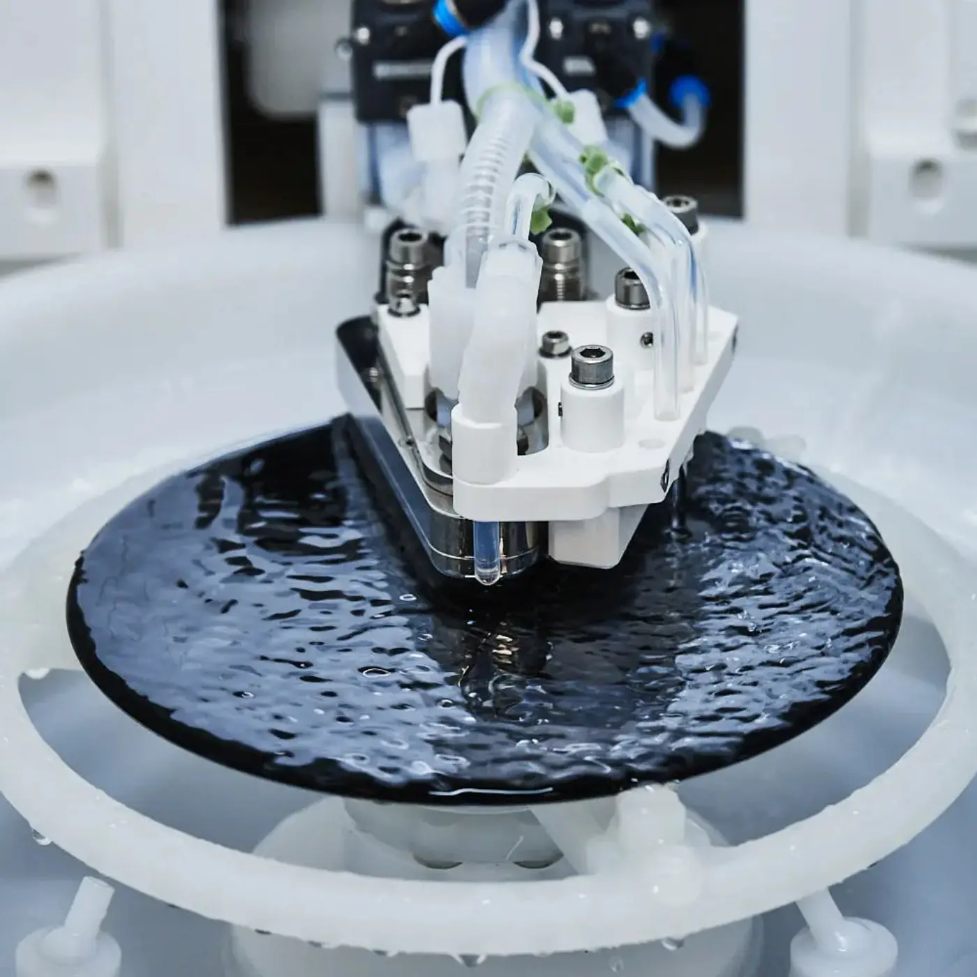
Manufacturer of wet process equipment for cleaning, etching and surface treatment of wafers in semiconductor manufacturing.

AP&S International GmbH
DresdenNew on Amplifa
About AP&S
AP&S International GmbH, headquartered in Dresden, develops and manufactures wet process equipment for wafer surface treatment. For more than 20 years, the company has supplied leading semiconductor manufacturers worldwide with equipment for batch and single-wafer processes as well as process-support equipment. The modular product portfolio covers processes such as cleaning, etching, photoresist stripping, development, metal etching, electroless plating, Marangoni drying and lift-off for wafers up to 300 mm in diameter. In addition to standard systems, custom solutions are offered; at the company's own wet process laboratory DemoLAB, process development and modification is performed, including for materials such as SiC, GaN-on-Si/SiC and InP. A comprehensive after-sales concept includes service visits, spare parts procurement, refurbishment, wet process training and the IoT portal AP&S WebWorker. For the third time in a row, AP&S won the productronica Innovation Award in the Semiconductor cluster, most recently with the fully automated box cleaner CleanSurF automated.
- Site
- Dresden
- Processes
- Wafer cleaning (wet cleaning with pure chemicals, batch and single wafer), Etching (wet etching of SC materials), Photoresist (PR) stripping, Development (resist development), Metal etching (Al, Ti, W and others), wafers up to 300 mm diameter, Electroless plating (under-bump metallization for flip-chip bonding), Wafer drying (Marangoni drying), Lift-off process (metal lift-off)
- Materials
- SiC, GaN-on-Si, GaN-on-SiC, InP, Aluminium, Titanium, Tungsten, Copper
- Industries
- Semiconductor industry, MEMS, Microelectronics
- 01
Process development and modification (DemoLAB)
- 02
Design and manufacturing of wet process equipment
- 03
Assembly and installation
- 04
Service visits and spare parts procurement
- 05
Refurbishment (modernization)
- 06
Wet process training (Academy)
- 07
Digitalization via IoT portal AP&S WebWorker
Materials & Processes
SiC (silicon carbide)
Semiconductor material for wet process development and demonstrations in the DemoLAB.
GaN-on-Si
Material system for process development in power electronics manufacturing.
GaN-on-SiC
Material system for innovative wet processes in semiconductor manufacturing.
InP (indium phosphide)
III-V semiconductor material for wet process demonstrations in the DemoLAB.
Aluminium
Metal for metal etching of device and monitor wafers up to 300 mm.
Titanium
Metal that is structured during wafer metal etching.
Tungsten
Metal for etching processes of metal structures on wafers.
Copper
Substrate material for electroless under-bump metallization.
Locations
Dresden
DECompany headquarters with Academy, consignment warehouse as well as development and manufacturing of wet process
- Materials
- SiC, GaN-on-Si, GaN-on-SiC, InP, Al, Ti, W, Cu
- CleanSurF automated (box cleaner)
- Wet process equipment for batch processes
- Wet process equipment for single-wafer processes
- DemoLAB wet process laboratory
Components
Inside the production
Industries
Processes & technical limits
| Processes | Tolerance | Max. part | Weight | Lot size | Materials |
|---|---|---|---|---|---|
| Wafer cleaning (wet cleaning with pure chemicals, batch and single wafer)Surface | – | – | – | – | Silicon wafers, SiC, GaN-on-Si, GaN-on-SiC, InP |
| Etching (wet etching of SC materials)Surface | – | – | – | – | Silicon wafers, SiC, GaN-on-Si, GaN-on-SiC, InP |
| Photoresist (PR) strippingSurface | – | – | – | – | – |
| Development (resist development)Surface | – | – | – | – | – |
| Metal etching (Al, Ti, W and others), wafers up to 300 mm diameterSurface | – | 300 mm (wafer diameter) | – | – | Aluminium, Titanium, Tungsten |
| Electroless plating (under-bump metallization for flip-chip bonding)Surface | – | – | – | – | Aluminum alloys, Copper |
| Wafer drying (Marangoni drying)Surface | – | – | – | – | – |
| Lift-off process (metal lift-off)Surface | – | – | – | – | – |
| Box cleaning (CleanSurF automated, multi-box cleaning)Surface | – | – | – | – | – |
| Process development and modification in the DemoLAB wet process laboratoryEngineering | – | – | – | – | SiC, GaN-on-Si, GaN-on-SiC, InP |
| Refurbishment (modernization of wet process equipment) and serviceEngineering | – | – | – | – | – |
3 Anlagen & Maschinen
| Machine | Manufacturer / model | Quantity | Working area | Year built | Site |
|---|---|---|---|---|---|
| Box cleaner (CleanSurF automated, fully automated) | AP&S CleanSurF automated | – | – | – | – |
| Wet process equipment for batch processes | AP&S | – | – | – | – |
| Wet process equipment for single-wafer processes | AP&S | – | – | – | – |
Additional services
History
Start of the delivery of wet process equipment for wafer surface treatment; more than 20 years in the market
- 2026
Relocation to the new site Manfred-von-Ardenne-Ring 13, Dresden (approx. 250 m from the previous location), with significantly enlarged spatial capacity for the Academy and the consignment warehouse
- 2026
Winning of the productronica Innovation Award (Semiconductor cluster) for the third time in a row, most recently with CleanSurF automated
- 2026
Participation in SEMICON Europa, 10–13 November 2026, booth B 1656