
Develops and manufactures wafer processing systems for thin-film deposition (ALD, epitaxy, PECVD) in semiconductor manufacturing.
ASM International N.V.
Almere (NL) · Phoenix/Scottsdale, Arizona (US) · Singapore (SG) · Helsinki (FI) · Leuven (BE) · Catania (IT)New on Amplifa
About ASM
ASM International N.V. is a Dutch company founded in 1968 by Arthur del Prado that develops and manufactures wafer processing systems for semiconductor manufacturing. The portfolio covers atomic layer deposition (ALD and PEALD), epitaxy for silicon, SiGe and silicon carbide (SiC), PECVD for dielectric films, and vertical batch furnaces for LPCVD, diffusion and oxidation. The processes enable ultra-thin, conformal films on 150-, 200- and 300-mm wafers for advanced logic, memory (DRAM/HBM), advanced packaging and SiC applications such as electric vehicles. The company employs more than 4,800 people at 15 key locations, more than 1,150 of them in research and development; manufacturing is centralized in Singapore. Headquarters are located in Almere (Netherlands), the largest R&D center in Phoenix/Scottsdale (Arizona, USA). Further R&D sites are Helsinki (materials and process research) and Leuven (partnership with IMEC), while the Catania (Italy) site has offered SiC epitaxy equipment since the LPE acquisition in 2022. ASM most recently invested around EUR 512 million in R&D and holds more than 3,950 patents.
- Site
- AP Almere
- Processes
- Atomic Layer Deposition (ALD), Thermal ALD, Plasma Enhanced ALD (PEALD), Epitaxy (crystalline film growth), SiC Epitaxy (Silicon Carbide), PECVD (Plasma-Enhanced Chemical Vapor Deposition), LPCVD (Low Pressure Chemical Vapor Deposition), Diffusion (doping)
- Materials
- Silicon (Si), Silicon Germanium (SiGe), Phosphorus-Doped Silicon (SiP), Silicon Carbide (SiC), Hafnium Oxide, Hafnium Silicate, Aluminum Oxide, Silicon Nitride
- Founded
- 1968
- Employees
- 4800+
- Industries
- Semiconductor manufacturing, Advanced logic/foundry, Memory (DRAM/HBM), Advanced packaging, SiC/electric vehicles, AI/data centers
- 01
R&D: materials & processes (Helsinki)
- 02
Process integration at partner institutes (including IMEC Leuven)
- 03
Product development for volume manufacturing
- 04
Centralized manufacturing (Singapore)
- 05
Installation & commissioning at the customer
- 06
Field service, spare parts & refurbishment
Technologies & Materials
Atomic Layer Deposition (ALD)
Ultra-thin, conformal films with angstrom-level control for advanced logic, memory and packaging.
Plasma Enhanced ALD
Plasma-enhanced deposition at lower temperatures for low-thermal-budget applications.
Epitaxy (Si, SiGe, SiP)
Crystalline film growth for channel and source/drain regions in advanced transistors.
SiC Epitaxy
Epitaxy equipment for silicon carbide, including for high-voltage applications and electric vehicles.
PECVD
Low-temperature dielectric deposition for advanced packaging and interconnects, including Flowable Carbon gap-fill.
Vertical Furnaces (LPCVD, Diffusion, Oxidation)
High-productivity batch processes for silicon, nitride, oxide and metal films.
Hafnium Oxide / Hafnium Silicate
High-k gate dielectrics for advanced CMOS transistors.
Silicon Nitride
Stress-tunable spacer and liner films for multiple patterning and packaging.
Aluminum Oxide
Fast, conformal passivation and dielectric films.
Flowable Carbon
Self-planarizing carbon film for void-free gap-fill of high aspect ratios.
Locations
Almere
NLHeadquarters (HQ)
Phoenix/Scottsdale (Arizona)
USLargest R&D center, offices
- New R&D center under construction (LEED certification targeted)
Singapore
SGCentralized manufacturing
Helsinki
FIR&D (materials and process research)
Leuven
BER&D (partner site IMEC)
Catania
ITSiC epitaxy (LPE, acquired 2022)
Systems & Products
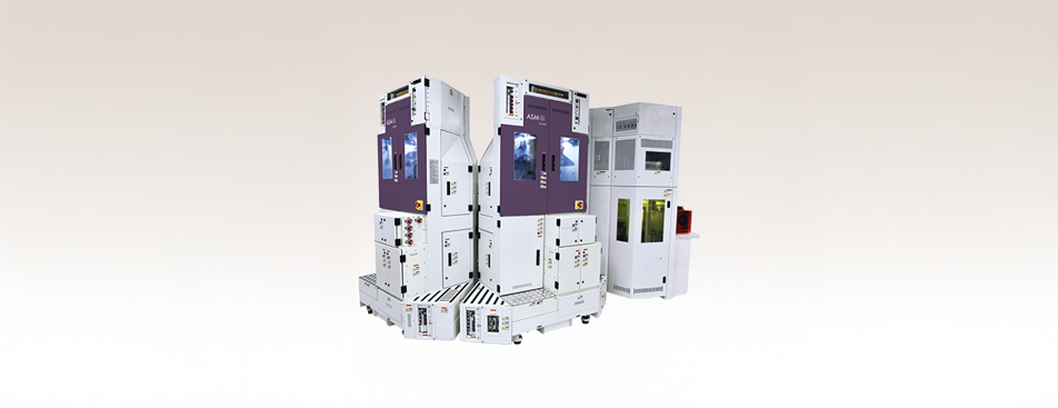

Inside the production
Industries
Processes & technical limits
| Processes | Tolerance | Max. part | Weight | Lot size | Materials |
|---|---|---|---|---|---|
| Atomic Layer Deposition (ALD)Surface | – | – | – | – | Oxides, Nitrides, Metals (ultra-thin films) |
| Thermal ALDSurface | – | – | – | – | Metal oxides, Dielectrics, Metal nitrides, Pure metals |
| Plasma Enhanced ALD (PEALD)Surface | – | – | – | – | SiO, SiN, TiO, Silicon nitride (SiN) |
| Epitaxy (crystalline film growth)Surface | – | – | – | – | Silicon (Si), Silicon germanium (SiGe), Phosphorus-doped silicon (SiP) |
| SiC Epitaxy (Silicon Carbide)Surface | – | – | – | – | Silicon carbide (SiC) |
| PECVD (Plasma-Enhanced Chemical Vapor Deposition)Surface | – | – | – | – | SiO, SiCN, SiN (stress-tunable), Flowable Carbon |
| LPCVD (Low Pressure Chemical Vapor Deposition)Surface | – | – | – | – | Pure silicon, doped silicon, silicon nitride, silicon oxides, metal films |
| Diffusion (doping)Heat treatment | – | – | – | – | Silicon |
| OxidationHeat treatment | – | – | – | – | Silicon |
| Surface Preclean (wafer cleaning)Surface | – | – | – | – | Silicon wafers |
| Flowable Carbon Gap-Fill and Planarization (PECVD)Surface | – | – | – | – | Flowable Carbon (carbon film) |
| Dry Cleaning (highly selective, acid-free)Surface | – | – | – | – | – |
| ALD Coating / Surface Modification / High-Precision RefurbishingSurface | – | – | – | – | – |
17 Anlagen & Maschinen
| Machine | Manufacturer / model | Quantity | Working area | Year built | Site |
|---|---|---|---|---|---|
| ALD process module (metal/dielectric ALD) | ASM XP4 EmerALD | – | – | – | – |
| ALD reactor (high-k) | ASM XP4 Pulsar (AXIS) | – | – | – | – |
| Thermal ALD system (up to 4 DCM, 8 chambers) | ASM XP8 Synergis | – | 300 mm | – | – |
| PEALD system (Dual Chamber Module, 8 chambers) | ASM XP8 DCM PEALD | – | 300 mm | – | – |
| PEALD system (Quad Chamber Module, 16 chambers) | ASM XP8 QCM PEALD | – | 300 mm | – | – |
| PEALD system (SiN deposition) | ASM XP8 JQCM PEALD | – | 300 mm | – | – |
| PEALD system | ASM XP8 Magma PEALD | – | 300 mm | – | – |
| Single-wafer epitaxy tool | ASM Epsilon 2000 | – | 150 mm and 200 mm wafers | – | – |
| Epitaxy deposition tool (300 mm) | ASM Intrepid ES / Intrepid ESA | – | 300 mm | – | – |
| Preclean module | ASM Previum (V3, NEXT, VP) | – | – | – | – |
| SiC epitaxy tool | ASM PE1O6A / PE1O8 | – | – | – | – |
| SiC epitaxy tool | ASM PE2O8 | – | – | – | – |
| PECVD system (Dual Chamber Module, 8 chambers) | ASM XP8 DCM PECVD | – | 300 mm | – | – |
| PECVD gap-fill/planarization system | ASM XP8 Vertos | – | – | – | – |
| Batch vertical furnace (300 mm, atmospheric/LP) | ASM SONORA | – | 300 mm | – | – |
| Batch vertical furnace (200 mm and smaller) | ASM A400 DUO | – | 200 mm and smaller wafers | – | – |
| Robotic system for precision maintenance (PM-bot) | ASM PM-bot | – | – | – | – |
Additional services
Company History
- 1968
ASM (Advanced Semiconductor Materials) was founded by Arthur del Prado in the Netherlands.
- 1970s
Furnace deposition manufacturing in the Netherlands; founding of ASM America (epitaxy base) and ASMPT in Hong Kong.
- 1980s
Founding of ASM Japan; participation in the Philips joint venture (today ASML), stake sold in 1988.
- 1990s
Focus on deposition; investments in ALD.
- 1999
Acquisition of ASM Microchemistry.
- 2004
Acquisition of ASM Genitech Korea.
- 2007
Pulsar ALD: first system in high-volume manufacturing with a hafnium-based high-k gate dielectric.
- 2013
Sale of the majority stake in ASMPT.
- 2022
Acquisition of LPE (Italy), entry into SiC epitaxy equipment; establishment of the Executive Committee.
- 2024
Hichem M'Saad appointed CEO; 100% renewable electricity for all global sites (H1 2024).
- 2025
Investor Day: target of revenue above EUR 5.7 billion and operating margin above 30% by 2030.