Manufacturer of lithography systems for the semiconductor industry and precision optics made of glass and ceramics
ASML Berlin AG
Veldhoven · Berlin · Dresden · Erlangen · Wilton, CT · San Diego, CA · Hillsboro, OR · Chandler, AZ · Silicon Valley, CA · Linkou · Hsinchu · Tainan · Hwaseong · Shanghai · Shenzhen · Beijing · TokyoNew on Amplifa
About ASML
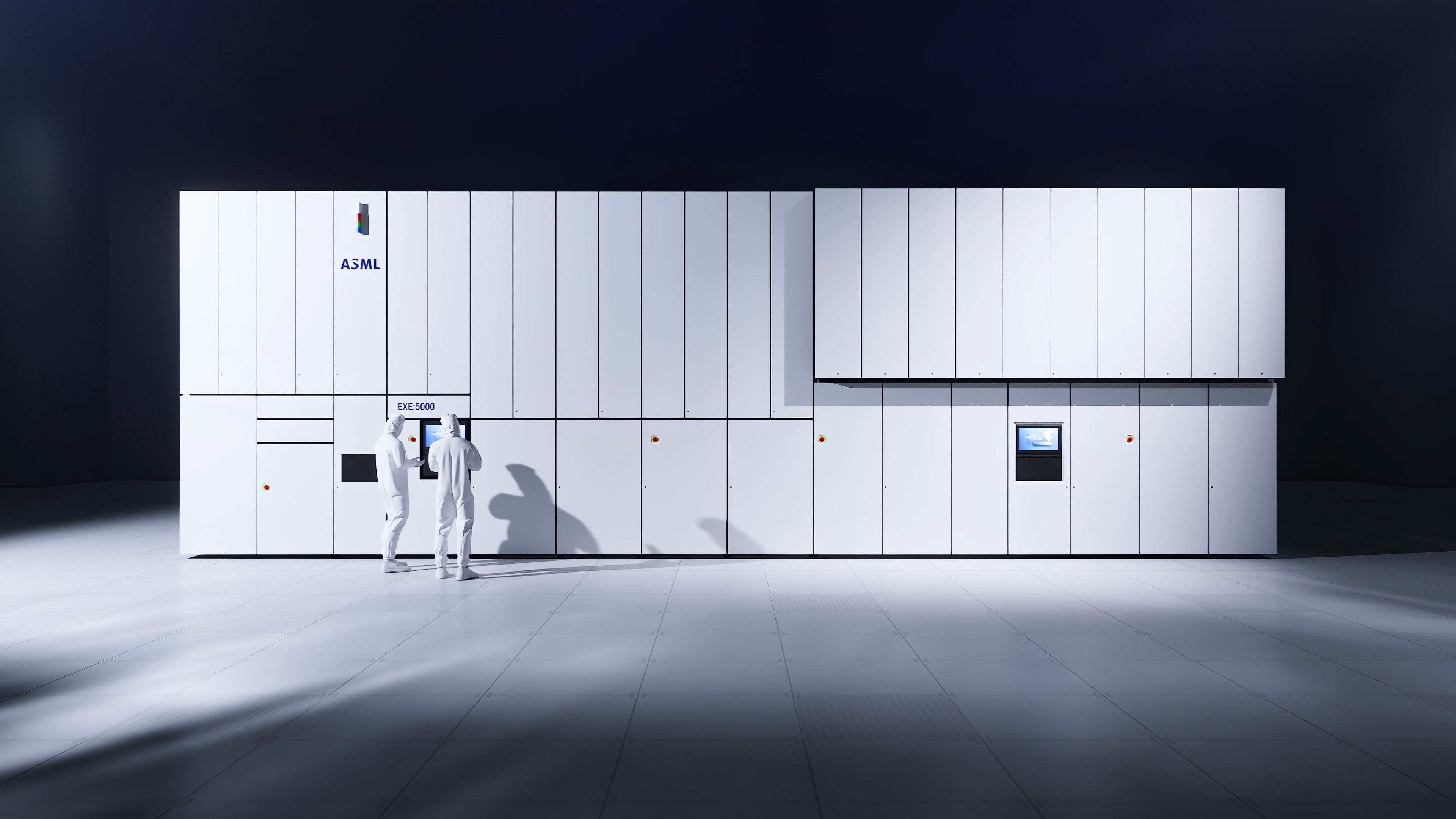
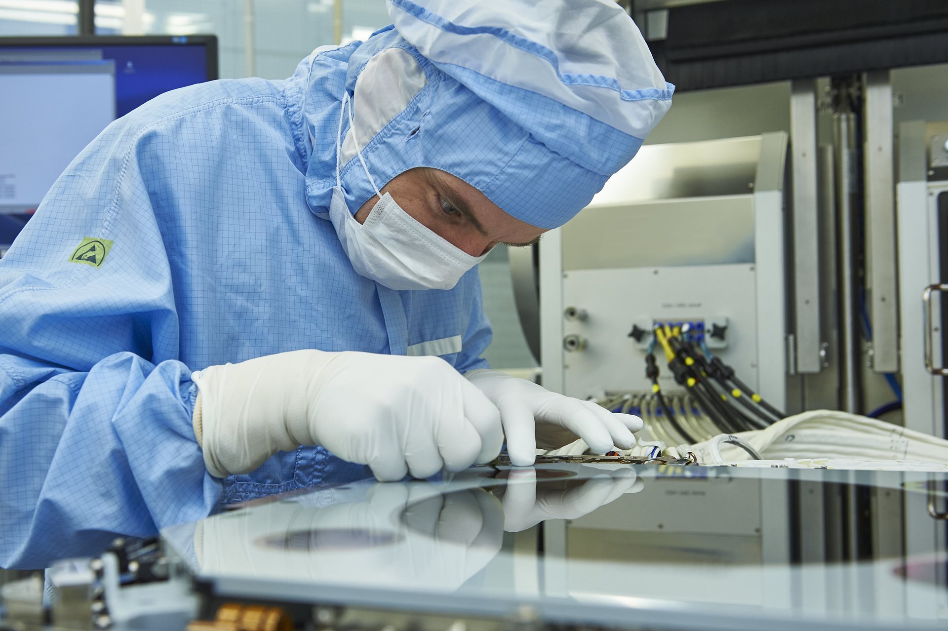
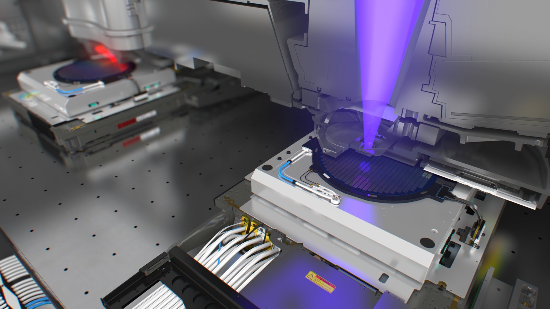
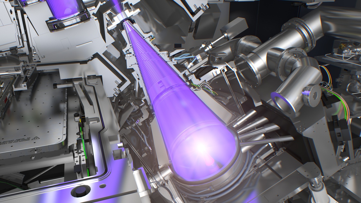
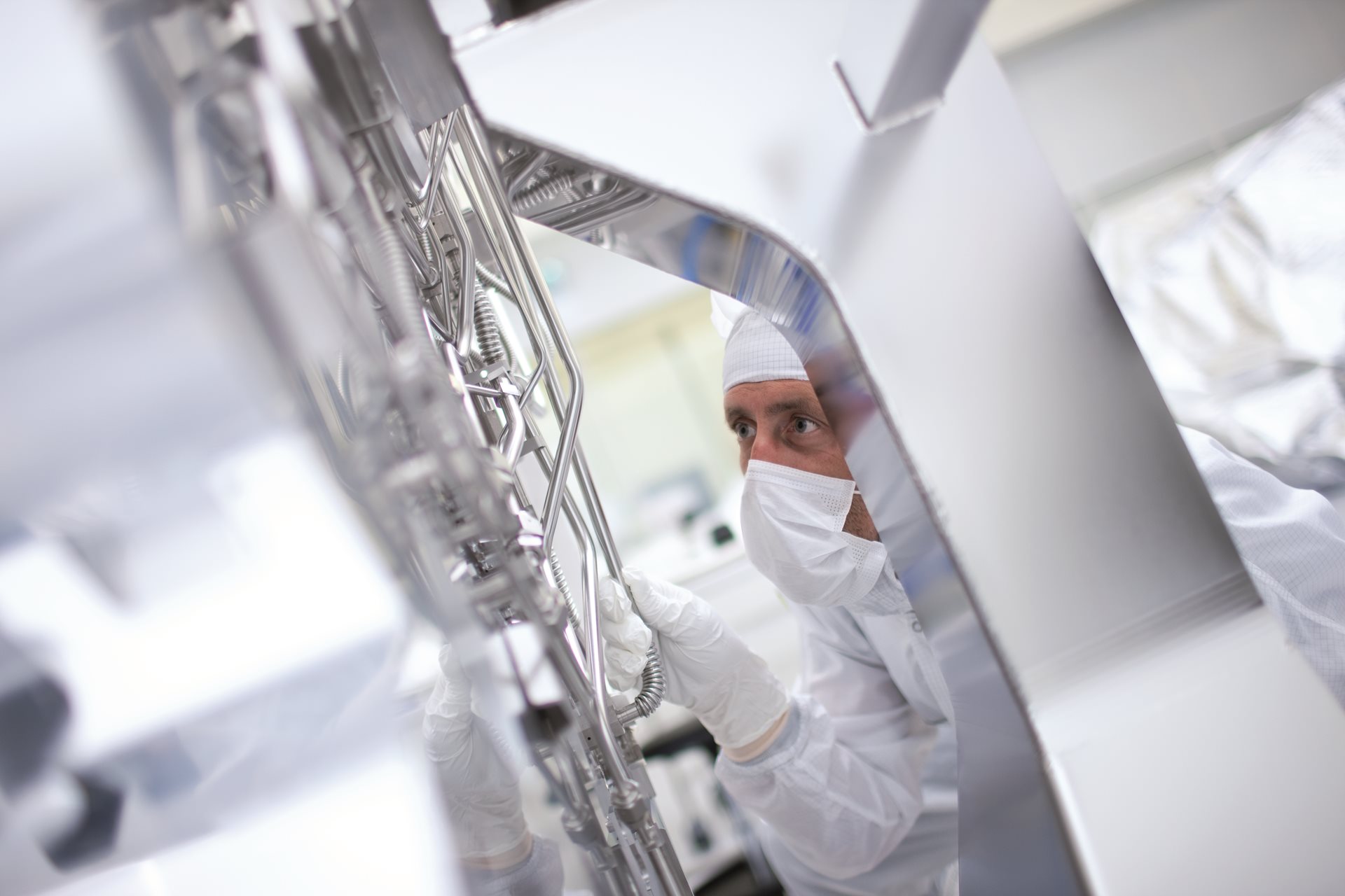
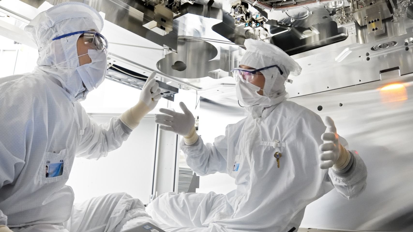
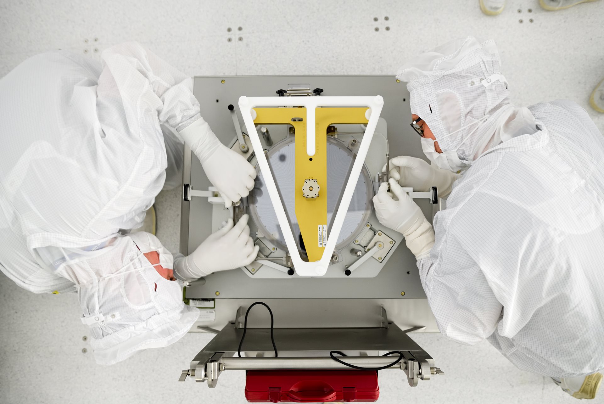
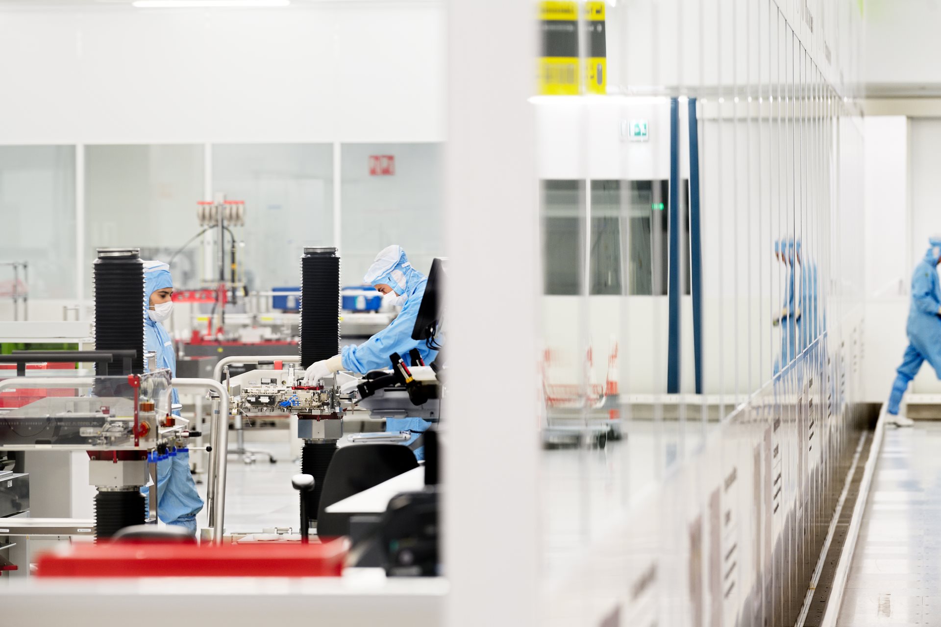
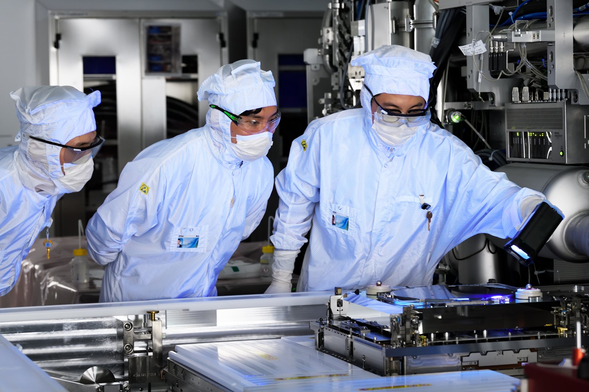
ASML is a Dutch technology group headquartered in Veldhoven that develops and manufactures lithography systems with which microchips are produced in series. The portfolio comprises DUV systems (193 nm), EUV lithography with a 13.5 nm wavelength and the High-NA EUV platform TWINSCAN EXE with a numerical aperture of 0.55. The systems are complemented by optical and e-beam metrology and inspection, computational lithography software as well as customer support in 14 countries. At the German site in Berlin (formerly Berliner Glas, acquired in 2020), more than 1,300 employees manufacture key components for lithography systems, including wafer tables, clamps, reticle chucks and mirror blocks made of glass, glass ceramic and ceramics – including CNC machining, cleanroom assembly, thin-film coating and optical-tactile metrology. Customers are the world's largest chipmakers such as TSMC, Samsung, Intel, SK Hynix and Micron.
- Site
- Berlin
- Processes
- EUV lithography (13.5 nm), High-NA EUV lithography (NA 0.55), DUV lithography (immersion and dry), Precision manufacturing of optical components made of glass, glass ceramic and ceramics, CNC machining of ceramic and glass-ceramic parts, Assembly/subassembly manufacturing under cleanroom conditions, Coating on thin-film systems (cleanroom), Joining of parts into assemblies
- Materials
- Silicon (wafers), Glass, Glass ceramic, Ceramics, Tin (EUV light source), Silicon, Tin
- Certificates
- Cleanroom manufacturing, Optical/tactile metrology (interferometers, 3D/4D measuring machines), Quality control in production
- Founded
- 1984
- Employees
- >44000
- Industries
- Semiconductor industry, Chip manufacturing (foundries, IDMs), Logic and memory chips
- 01
Development and R&D
- 02
CNC machining of ceramic and glass-ceramic parts
- 03
Manufacture of optical components
- 04
Coating on thin-film systems
- 05
Cleanroom assembly and joining into assemblies
- 06
Optical and tactile metrology
- 07
EUV/DUV lithography systems, metrology and software
- 08
Customer support and refurbishment
Materials & Processes
Glass
Base material for highly precise optical components and assemblies of the lithography systems.
Glass ceramic
Machined in Berlin into dimensionally stable precision parts such as wafer tables and mirror blocks.
Ceramics
CNC-machined ceramic parts for clamps, reticle chucks and other precision components.
Silicon
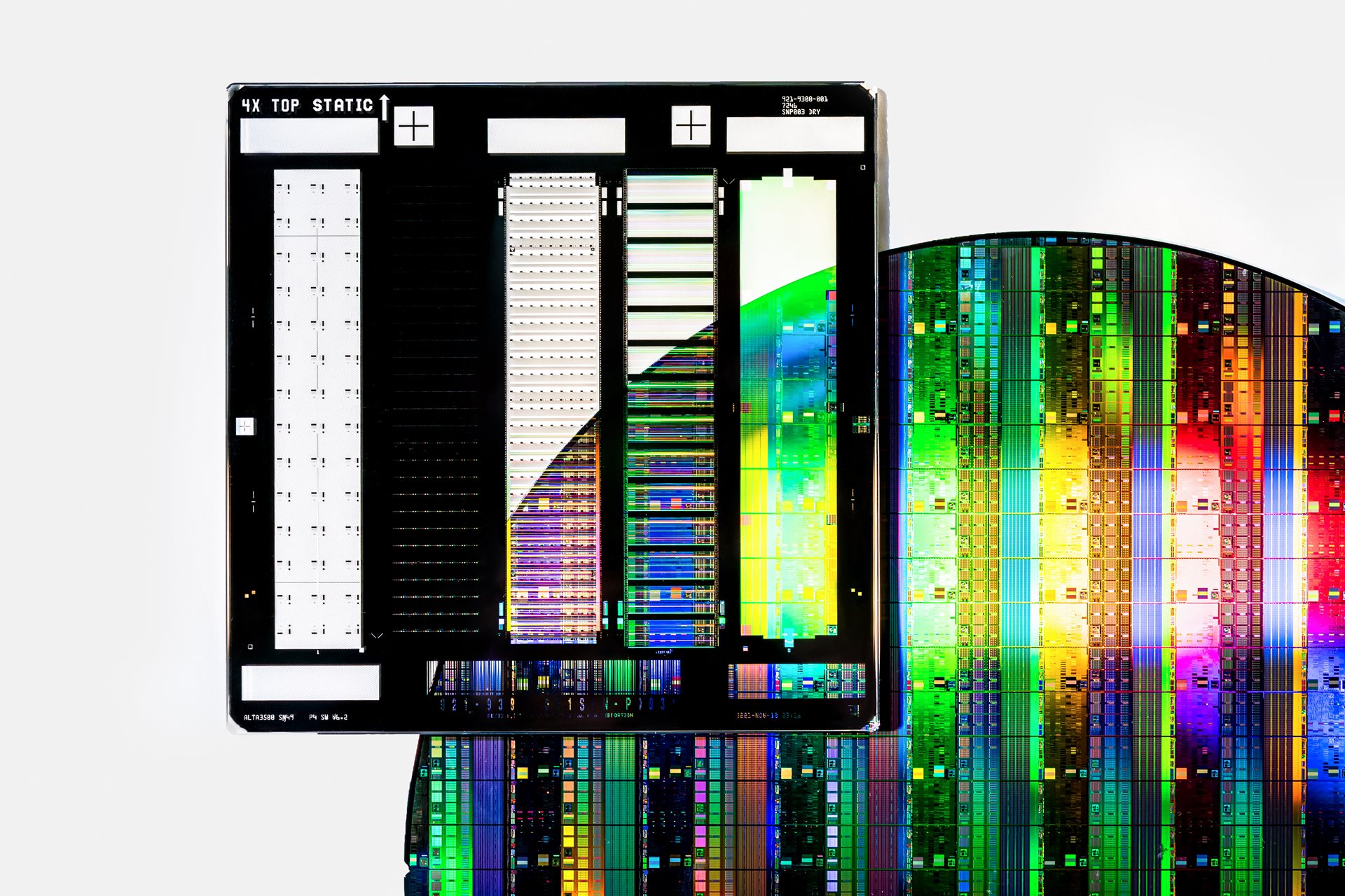
Material of the wafers onto which the lithography systems project the chip structures.
Tin
Droplets of molten tin form the laser-generated plasma source of the EUV light source (13.5 nm).
Parts & Components
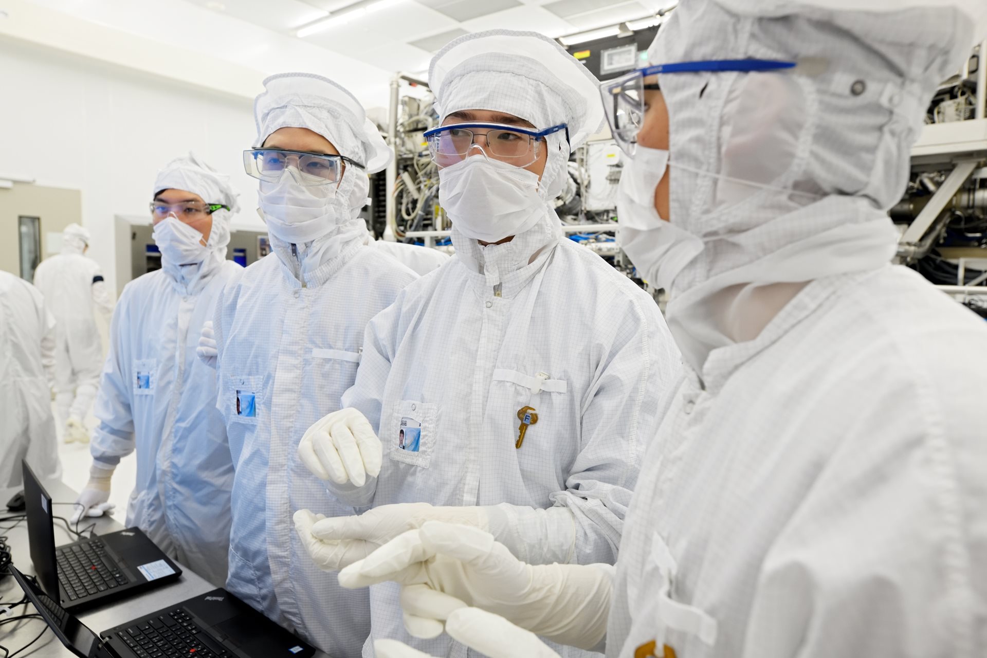
Inside the production


Industries
Processes & technical limits
| Processes | Tolerance | Max. part | Weight | Lot size | Materials |
|---|---|---|---|---|---|
| EUV lithography (13.5 nm)Other | – | – | – | – | Silicon |
| High-NA EUV lithography (NA 0.55)Other | – | – | – | – | Silicon |
| DUV lithography (immersion and dry)Other | – | – | – | – | Silicon |
| Precision manufacturing of optical components made of glass, glass ceramic and ceramicsMachining | – | – | – | – | Glass, Glass ceramic, Ceramics |
| CNC machining of ceramic and glass-ceramic partsMachining | – | – | – | – | Ceramics, Glass ceramic |
| Assembly/subassembly manufacturing under cleanroom conditionsAssembly | – | – | – | – | Glass, Glass ceramic, Ceramics |
| Coating on thin-film systems (cleanroom)Surface | – | – | – | – | Glass, Glass ceramic, Ceramics |
| Joining of parts into assembliesJoining | – | – | – | – | Glass, Glass ceramic, Ceramics |
| Optical and tactile metrology (interferometers, 3D/4D measuring machines)Testing | – | – | – | – | Glass, Glass ceramic, Ceramics |
| E-beam metrology and inspectionTesting | – | – | – | – | Silicon |
| Refurbishment of PAS 5500 and TWINSCAN lithography systemsEngineering | – | – | – | – | – |
10 Anlagen & Maschinen
| Machine | Manufacturer / model | Quantity | Working area | Year built | Site |
|---|---|---|---|---|---|
| EUV lithography system (NXE) | ASML NXE | – | NA 0.33, 13.5 nm wavelength | – | Veldhoven, Netherlands |
| High-NA EUV lithography system | ASML TWINSCAN EXE:5000 | – | NA 0.55, 13.5 nm wavelength, >185 wafers/h | – | Veldhoven, Netherlands |
| DUV lithography system (immersion and dry) | ASML | – | 193 nm wavelength | – | Veldhoven, Netherlands |
| CNC machines for machining ceramics/glass ceramic | – | – | – | – | Berlin, Germany |
| Interferometers, 3D and 4D measuring machines | – | – | – | – | Berlin, Germany |
| Thin-film coating systems (cleanroom) | – | – | – | – | Berlin, Germany |
| E-beam inspection systems | ASML (HMI) | – | – | – | Tainan, Taiwan / Beijing, China |
| YieldStar metrology systems (manufacturing) | ASML YieldStar | – | – | – | Linkou, Taiwan |
| Reticle handlers (manufacturing) | ASML | – | – | – | Linkou, Taiwan |
| DUV/EUV light sources (Cymer) | Cymer (ASML) | – | – | – | San Diego, CA, USA |
Additional services
Reference customers
Quality & Measurement Accuracy
The components made of glass, glass ceramic and ceramics are inspected with optical and tactile measuring equipment such as interferometers as well as 3D and 4D measuring machines. On the system side, the wafer stage is controlled and adjusted 20,000 times per second to a quarter-of-a-nanometer accuracy.
| Evidence | Berlin | Veldhoven |
|---|---|---|
| Cleanroom manufacturing | ||
| Optical/tactile metrology (interferometers, 3D/4D measuring machines) | ||
| Quality control in production |
Company History
- 1984
Founded as a joint venture of Philips and ASM International in Veldhoven ("ASM Lithography") with around 100 employees; first system PAS 2000
- 1986
First competitive wafer stepper system PAS 2500; start of collaboration with Carl Zeiss SMT
- 1988
ASM International withdraws, Philips takes over; expansion to Taiwan and the USA
- 1991
Introduction of the PAS 5500 – first major commercial breakthrough
- 1995
IPO on the Amsterdam and New York stock exchanges (March 15)
- 1997
Start of EUV research and development
- 2000
Acquisitions of MaskTools and Silicon Valley Group (SVG); more than 8,000 employees
- 2007
Acquisition of BRION; first holistic lithography approach
- 2010
First EUV platform NXE shipped
- 2012
Intel invests USD 4.1 billion for a 15% stake to finance EUV development; Samsung and TSMC also take stakes
- 2013
Acquisition of Cymer (light sources for lithography)
- 2016
Acquisition of Hermes Microvision (HMI, e-beam inspection)
- 2017
Quasi-monopoly in EUV lithography as the only manufacturer worldwide
- 2020
Acquisition of optics manufacturer Berliner Glas completed (today ASML Berlin)
- 2023
Delivery of the first modules of the first High-NA EUV system TWINSCAN EXE:5000 to Intel (December)
- 2025
Stake of over EUR 1.3 billion (11%) in the software developer Mistral AI
- 2026
Largest known single order from SK Hynix worth almost EUR 7 billion; High-NA platform EXE with NA 0.55 in delivery