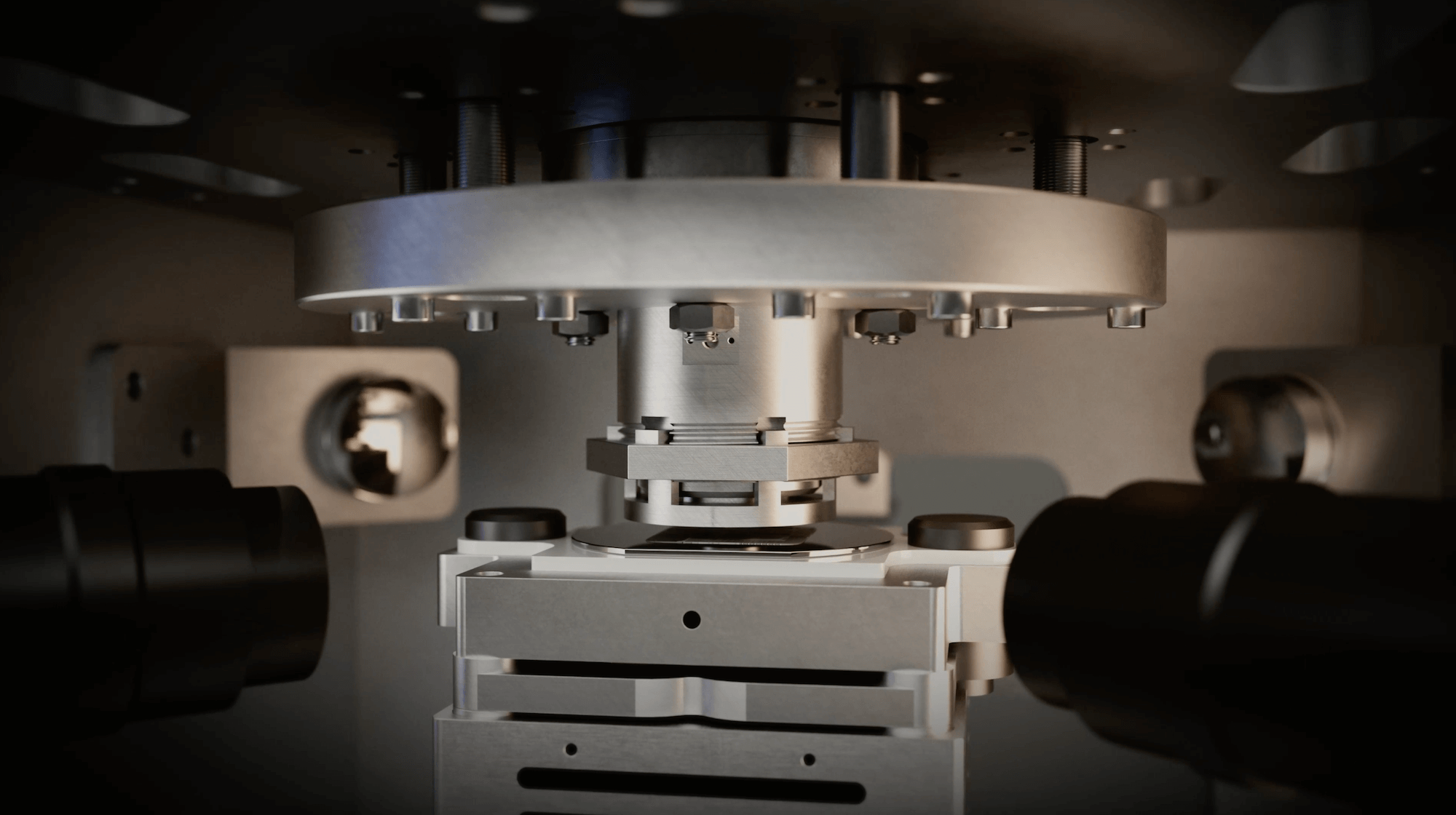
ATLANT 3D manufactures micro- and nanocomponents for microelectronics and photonics using atomically precise DALP® deposition technology

ATLANT 3D
Location not specifiedNew on Amplifa
About ATLANT 3D
ATLANT 3D is a company for atomically precise advanced manufacturing that provides digital and atomically precise process technologies along the entire microelectronics value chain. At its core is the company's proprietary DALP® technology (Direct Atomic Layer Processing), a microreactor-based deposition technology with atomic precision capable of processing more than 450 materials – including silicon, gallium, indium, germanium and copper. The service portfolio ranges from advanced materials research and prototyping of micro- and nanodevices (MEMS/sensors, microfluidics, RF, optical and photonic devices) to scalable manufacturing. For research and industry, ATLANT 3D offers the NANOFABRICATOR™ product series: LITE for academia and research (sample size up to 100 mm, line widths down to 100 µm, deposition speed up to 200 mm/s, up to two materials simultaneously), PRO for industrial R&D, as well as ZERO-G. The technology is low-waste and chemical-reduced and is compatible with semiconductor industry standards. Application areas include optics & photonics, sensors & MEMS, advanced packaging & semiconductor manufacturing, biotechnology & medical devices, energy technology, and RF & printed electronics.
- Site
- Location not specified
- Processes
- DALP® – Direct Atomic Layer Processing (atomic material deposition), Prototyping of micro- and nanodevices (MEMS, microfluidics, RF, optical/photonic devices), Edge passivation for highly efficient solar cells (ACES project), Innovation Services, Atomically precise material deposition (DALP®), Prototyping of micro- and nanodevices, Scalable manufacturing
- Materials
- Silicon, Gallium, Indium, Germanium, Copper (for solar cell metallization), Silver (reference material to be replaced in solar cell metallization), Direct Atomic Layer Processing, Copper
- Industries
- Optics & Photonics, Sensors & MEMS, Advanced Packaging & Semiconductor Fabrication, Biotechnology & Medical Devices, Energy Technology (Batteries, Fuel Cells, Catalysis), RF & Printed Electronics
- 01
Materials research (Advanced Materials R&D)
- 02
DALP® atomic material deposition
- 03
Prototyping of micro- and nanodevices
- 04
Scalable manufacturing
- 05
Application-specific integration (optics, photonics, MEMS/sensors)
Materials and Processes
Direct Atomic Layer Processing
Microreactor-based deposition technology with atomic precision for microelectronics and photonics, capable of processing more than 450 materials.
Silicon
Semiconductor material for microelectronics and solar cell applications such as edge passivation.
Gallium
Processable material of DALP® technology, among other things for compound semiconductors.
Indium
Processable material of DALP® technology for micro- and nanodevices.
Germanium
Processable material of DALP® technology for semiconductor and photonics applications.
Copper
Material for solar cell metallization as a substitute for silver.
Locations
Location not specified
Development and manufacturing of the NANOFABRICATOR series
- Materials
- more than 450 materials (DALP®)
- NANOFABRICATOR™ LITE
- NANOFABRICATOR™ PRO
- NANOFABRICATOR® ZERO-G
Components and Applications


Inside the production



Industries
Processes & technical limits
| Processes | Tolerance | Max. part | Weight | Lot size | Materials |
|---|---|---|---|---|---|
| DALP® – Direct Atomic Layer Processing (atomic material deposition)Additive | atomic precision (details not specified) | Sample size up to 100 mm | – | – | more than 450 materials processable, Silicon, Gallium, Indium, Germanium, Copper |
| Prototyping of micro- and nanodevices (MEMS, microfluidics, RF, optical/photonic devices)Engineering | Line Width down to 100 µm (NANOFABRICATOR LITE) | 100 mm | – | – | – |
| Edge passivation for highly efficient solar cells (ACES project)Surface | – | – | – | – | Silicon, Copper (silver substitution in metallization) |
3 Anlagen & Maschinen
| Machine | Manufacturer / model | Quantity | Working area | Year built | Site |
|---|---|---|---|---|---|
| NANOFABRICATOR™ LITE (atomic deposition tool for research/academia) | ATLANT 3D NANOFABRICATOR LITE | – | Sample size up to 100 mm; Line Width down to 100 µm; Deposition speed up to 200 mm/s; up to 2 | – | – |
| NANOFABRICATOR™ PRO (Industrial R&D tool) | ATLANT 3D NANOFABRICATOR PRO | – | – | – | – |
| NANOFABRICATOR® ZERO-G | ATLANT 3D NANOFABRICATOR ZERO-G | – | – | – | – |
Additional services
History
- 2024
Launch of the EU-funded ACES project (Horizon Europe, budget EUR 3.5 million) in April 2024, among other things for edge passivation for highly efficient solar cells.
- 2024
Launch of the EU-funded CLOSER project (Horizon Europe, budget EUR 14 million) in October 2024 to build a European circular economy supply chain for semiconductor raw materials.