
Develops and manufactures integrated cathodoluminescence systems for non-destructive defect inspection of semiconductors and wafers.

Attolight AG
Ecublens (Switzerland) · Cambridge, MA (USA)New on Amplifa
About Attolight
Attolight is a Swiss company founded in 2008 and headquartered in Ecublens that develops and manufactures cathodoluminescence (CL) instruments for materials characterization and defect inspection. The company is the only supplier of fully integrated CL systems in which electron optics and light optics are jointly designed and optimized. The portfolio comprises the multi-spectroscopic CL-SEM platform Allalin, the CL add-on for STEM (Mönch) and the full-wafer CL-SEM system Säntis 300; the Allalin Chronos system enables time-resolved CL measurements in the picosecond range. The technology is used, among others, by semiconductor manufacturers and research institutes in the fields of optoelectronics, data communications, quantum technologies, life science and energy materials; more than 30 systems are installed worldwide. In addition to its equipment business, Attolight offers measurement services, maintenance and support as well as specific development and engineering services.
- Site
- Ecublens
- Processes
- Cathodoluminescence (CL) Defect Inspection / Materials Characterization, Panchromatic CL Imaging, Cathodoluminescence Spectroscopy, Quantitative Cathodoluminescence (q-CL), Time-Resolved Cathodoluminescence (TRCL, <10ps), EBIC/EBAC Imaging, Degree of Polarization (DoP) CL, Hyperspectral Imaging
- Materials
- Phosphide semiconductors (InP), Nitride semiconductors (GaN, InGaN), Silicon carbide (SiC), Silicon and alloys, Oxide semiconductors (ZnO, SnO2), II-VI semiconductors (CdTe, CdS, CIGS), Transition metal dichalcogenides, Halide perovskites
- Certificates
- Global support network with guaranteed response times, Certifications (e.g. ISO 9001)
- Founded
- 2008
- Industries
- Semiconductors, Optoelectronics, Data communications, Quantum technologies, Life science, Energy materials (photovoltaics, thin-film batteries)
- 01
R&D and development of electron and light optics
- 02
Equipment manufacturing and system integration
- 03
Measurement services
- 04
Maintenance, support and engineering services
Locations
Ecublens
CHHead office (HQ), R&D and equipment manufacturing
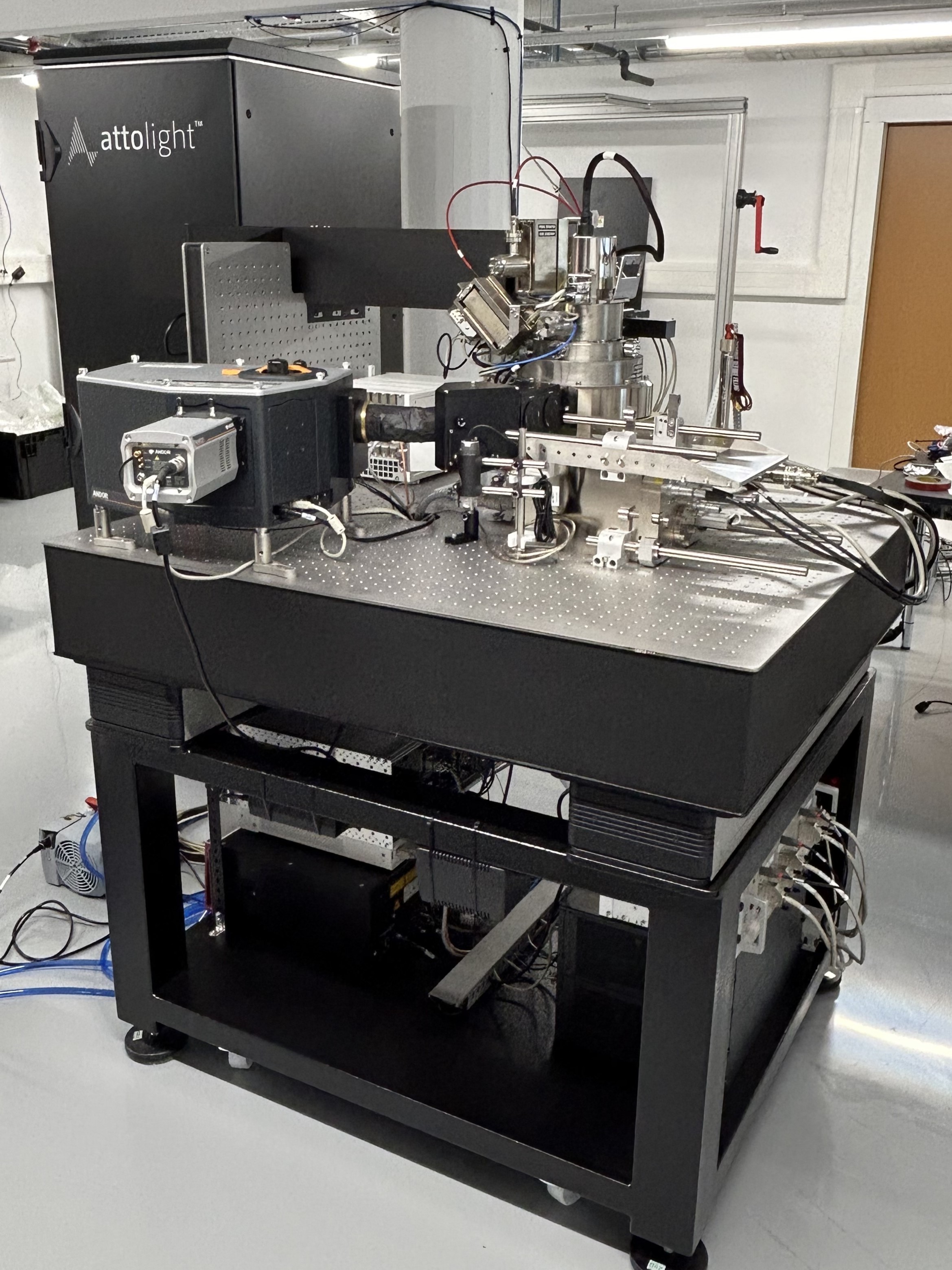
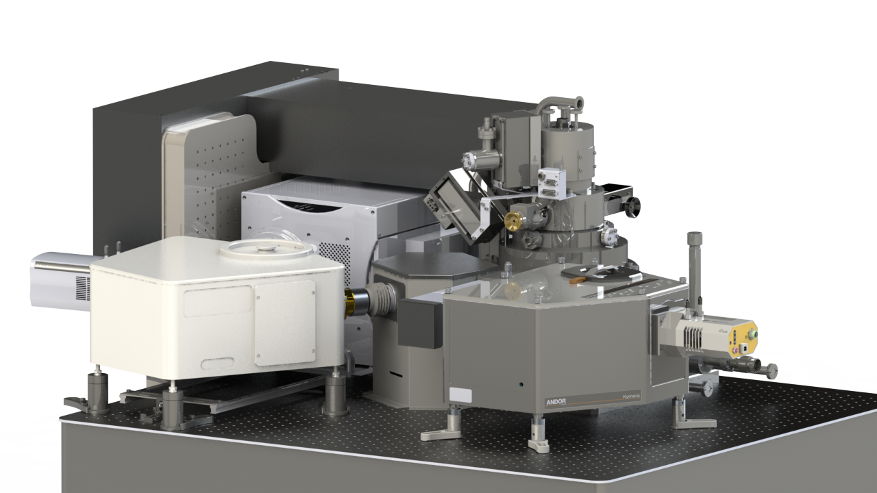
- Allalin – Multi Spectroscopic CL SEM Platform
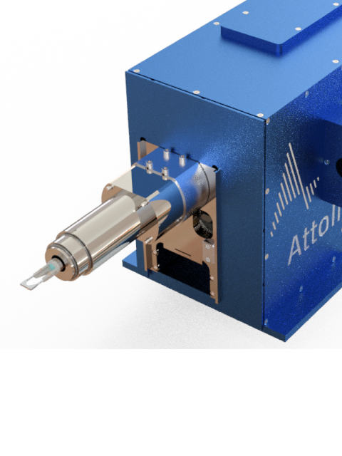
- Mönch – CL Add-On for STEM
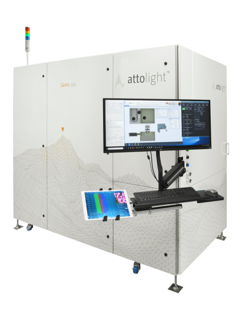
- Säntis 300 – Full Wafer CL SEM
- Allalin Chronos – Time-Resolved CL
Cambridge, MA
USSubsidiary for the North American market (service and support)
Products
Inside the production
Industries
Processes & technical limits
| Processes | Tolerance | Max. part | Weight | Lot size | Materials |
|---|---|---|---|---|---|
| Cathodoluminescence (CL) Defect Inspection / Materials CharacterizationTesting | – | – | – | – | Semiconductors, Optoelectronic materials, Inorganic materials, Nitride semiconductors, Phosphide semiconductors, Arsenide semiconductors, Oxide semiconductors, Silicon carbide, Silicon and alloys, Diamond, II-VI semiconductors, Transition metal dichalcogenides, Halide perovskites, Rare-earth doped phosphors, Polymers & Biopolymers, Plasmonic/metamaterials |
| Panchromatic CL ImagingTesting | – | – | – | – | Nitride semiconductors, Phosphide semiconductors, Silicon carbide |
| Cathodoluminescence SpectroscopyTesting | – | – | – | – | Semiconductors, Optoelectronic materials |
| Quantitative Cathodoluminescence (q-CL)Testing | – | – | – | – | Nitride semiconductors, Phosphide semiconductors, Halide perovskites |
| Time-Resolved Cathodoluminescence (TRCL, <10ps)Testing | – | – | – | – | Halide perovskites, Nitride semiconductors, Oxide semiconductors |
| EBIC/EBAC ImagingTesting | – | – | – | – | Semiconductors |
| Degree of Polarization (DoP) CLTesting | – | – | – | – | Semiconductors |
| Hyperspectral ImagingTesting | – | – | – | – | Transition metal dichalcogenides, Oxide semiconductors, Halide perovskites |
| Cathodoluminescence g(2) AutocorrelationTesting | – | – | – | – | – |
| In-SEM Electrical Probing (Nanoprobing)Testing | – | – | – | – | Semiconductors |
| Cryogenic Cathodoluminescence (Cryo-CL, down to 10 K)Testing | – | – | – | – | Semiconductors |
| In-SEM Raman spectroscopyTesting | – | – | – | – | – |
| CL-STEM (Correlative STEM-CL)Testing | – | – | – | – | hBN, Halide perovskites |
| Measurement Services (CL analyses as a service)Testing | – | – | – | – | Semiconductors, Optoelectronic materials, Inorganic materials |
| Custom Equipment Design / Software CustomizationEngineering | – | – | – | – | – |
| Maintenance and Support ServicesEngineering | – | – | – | – | – |
4 Anlagen & Maschinen
| Machine | Manufacturer / model | Quantity | Working area | Year built | Site |
|---|---|---|---|---|---|
| Multi Spectroscopic CL SEM Platform | Attolight Allalin | – | – | – | Ecublens, Switzerland (HQ) |
| CL Add-On for STEM | Attolight Mönch | – | – | – | – |
| Full wafer CL SEM | Attolight Säntis 300 | – | Full wafer | – | – |
| Allalin Chronos TRCL (Time-Resolved CL) | Attolight Allalin Chronos | – | – | – | – |
Additional services
Reference customers
Quality & Support
The proprietary, patented optical designs ensure reproducible and quantitative measurements without intensity or resolution artefacts. A global support network with local engineers, guaranteed response times and spare parts stocks ensures system operation.
| Evidence | Ecublens |
|---|---|
| Global support network with guaranteed response times | |
| Certifications (e.g. ISO 9001) |
History
- 2008
Attolight was founded by Samuel Sonderegger.
Transformation of the products from manual laboratory and FA tools to full-wafer semiconductor fab solutions; more than 30 systems installed worldwide.