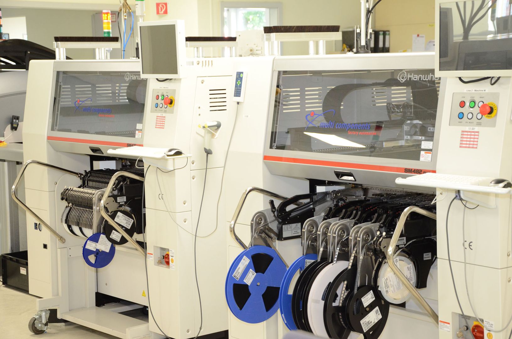
Development and population of electronic assemblies: SMD and THT manufacturing, vapor phase and selective soldering as well as cable assembly in Heßdorf.

Birkholz Elektronische Geräte GmbH
Heßdorf (Bavaria)New on Amplifa
About Birkholz Elektronische Geräte GmbH
Birkholz Elektronische Geräte GmbH is an EMS provider for industrial electronics based in Heßdorf near Erlangen. Founded in 1980, the company develops and populates printed circuit boards in SMD and THT technology, including fine-pitch and BGA components, and manufactures in very small, small and medium-sized series. The value chain covers electronic development, component purchasing, SMD population with seven placement machines from Hanwha and Samsung, vapor phase soldering (including vacuum phase), lead-free selective and wave soldering, AOI inspection, functional testing, washing, coating, potting, cable assembly and final assembly. A fully automated SMD dry storage system (KLS) stores components IPC-compliant at 40 °C and below 5 % relative humidity. Weekly capacity exceeds 1.5 million placed components in multi-shift operation. Customers come from control and automation technology, power electronics, medical technology, mining, radiation measurement technology and LED lighting technology for rail vehicles. Since January 2024, the company has been part of KRIWAN Holding (Forchtenberg). On approximately 2,600 m² of production space in Heßdorf, the company manufactures for customers in Bavaria, Baden-Württemberg and Hesse.
- Site
- Heßdorf
- Processes
- SMD population (single- and double-sided, 1.5 million components/week), Automated snap-in population, Conventional (THT) population / re-population, Vapor phase soldering, Vapor phase soldering vacuum (gas inclusion reduction), Inline vapor phase soldering (up to 6 panels), Selective soldering (lead-free, nitrogen), Lead-free wave soldering
- Materials
- Printed circuit boards (single-/double-sided), Printed circuit boards flexible/semi-flexible, Printed circuit boards plated-through, Multilayer printed circuit boards, Aluminium printed circuit boards, Teflon printed circuit boards, Lead-free solder, Single- and double-sided printed circuit boards
- Certificates
- DIN EN ISO 9001:2015, UL Recognized Component (Z353, UL 796), ISO 9001, UL Recognized Component (Z353)
- Founded
- 1980
- Industries
- Control and automation technology, Power electronics, Medical technology, Mining, LED lighting technology for rail vehicles, Radiation measurement technology
- 01
Electronic development
- 02
Component purchasing / material procurement
- 03
SMD dry storage
- 04
SMD and THT population
- 05
Vapor phase, selective and wave soldering
- 06
AOI inspection and visual inspection
- 07
Washing, coating, potting
- 08
Functional testing
- 09
Cable assembly and final assembly
Printed circuit boards and materials
Single- and double-sided printed circuit boards
Standard manufacturing for SMD and THT population in small and medium-sized series.
Flexible and semi-flexible printed circuit boards
For applications with moving or curved assemblies.
Plated-through printed circuit boards
Standard for multi-layer electrical through-connections.
Multilayer printed circuit boards
For complex assemblies with high trace density.
Aluminium printed circuit boards
For power electronics with high thermal requirements.
Teflon printed circuit boards
For high-frequency applications with special dielectric properties.
Lead-free solder
Used in the selective soldering process under nitrogen atmosphere.
Vapor phase soldering
Oxygen-free soldering process, ideally suited for BGA and fine-pitch components.
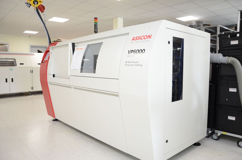
Vapor phase soldering with vacuum phase (VP6000)
Reduces gas inclusions in solder joints, among other things to improve current-carrying capacity.
Selective soldering (lead-free, nitrogen)
For high-mass printed circuit boards, nozzles from 3 mm diameter.
Lead-free wave soldering
In use since 2008 for series production.
Heßdorf site
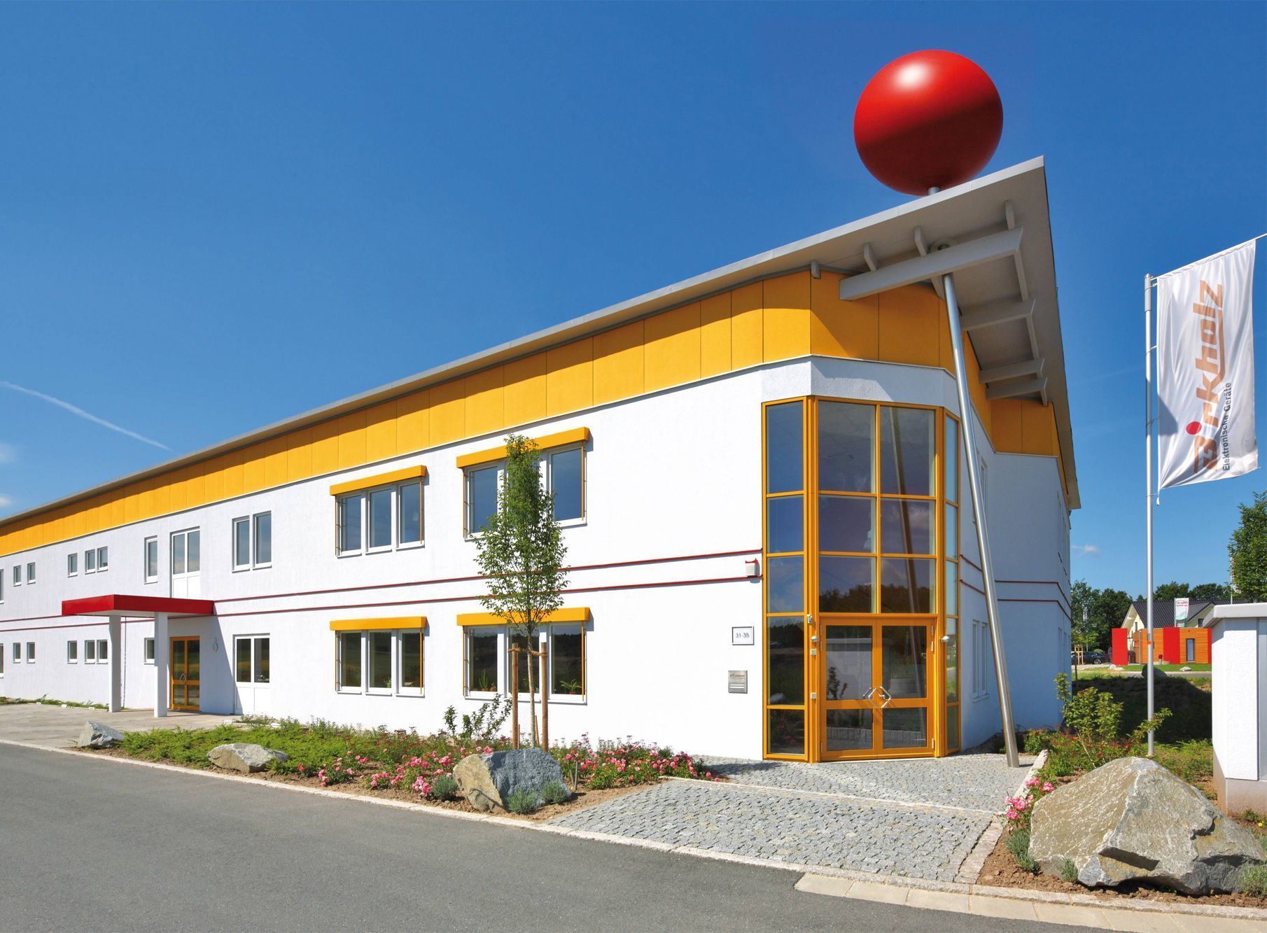
Heßdorf
DEManufacturing, development, administration
- Lot size
- Very small, small and medium-sized series
- Materials
- Printed circuit boards (single-/double-sided, flexible, multilayer, aluminium, Teflon), lead-free solder
- 7x Hanwha/Samsung SMD placement machines (SM471plus, SM481, SM482plus, SM485, SM411, 2x SM421)
- 3x DEK solder paste printers (Horizon 01iX, Horizon 03iX, Infinity)
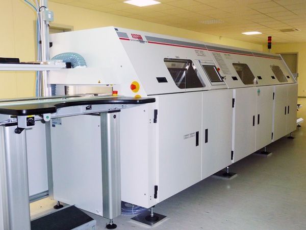
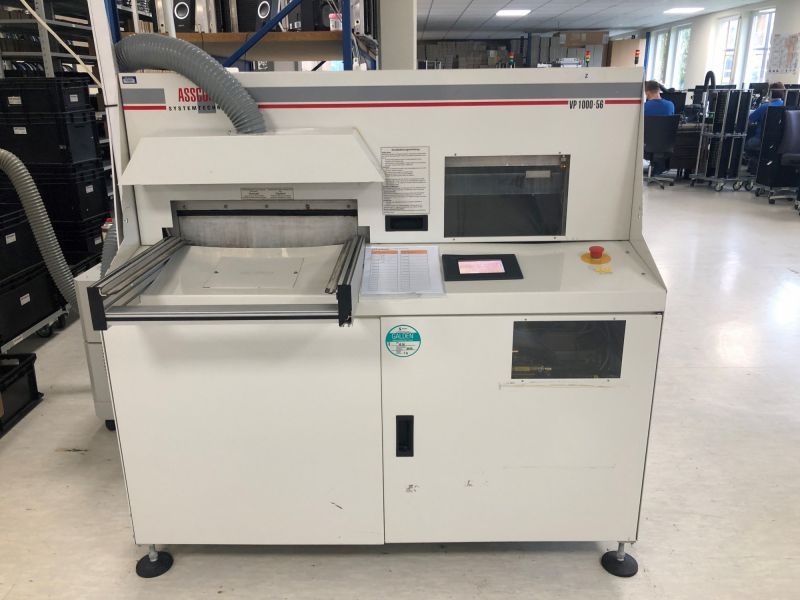
- 3x Asscon vapor phase soldering systems (VP56, VP2000 Inline, VP6000 Vacuum)
- Ersa inline selective soldering system Versaflow (Versaflex, 2 pots)
- Seho selective soldering system
- Lead-free wave soldering system
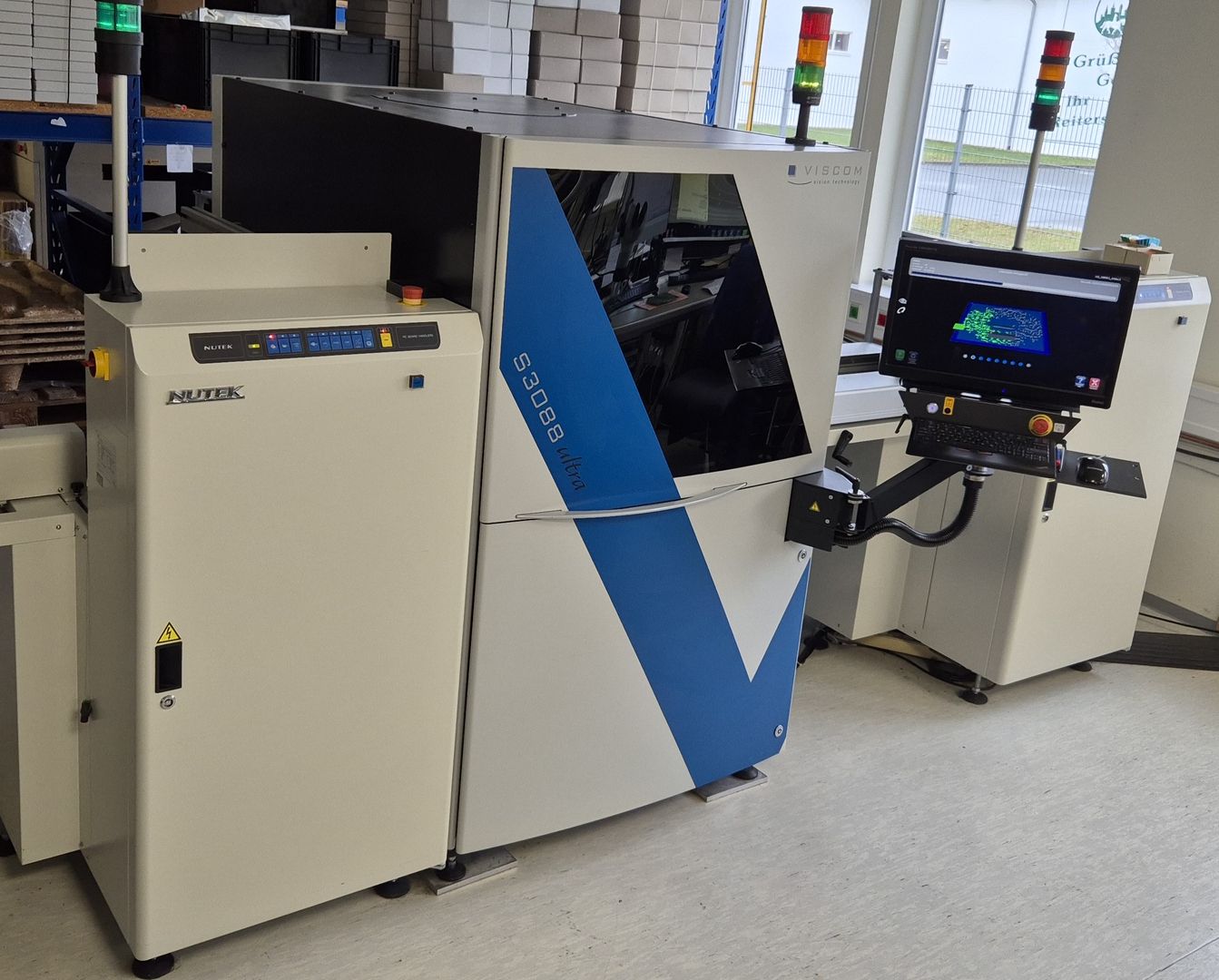
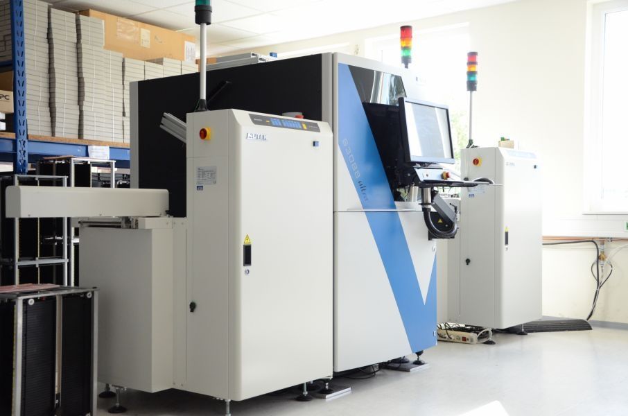
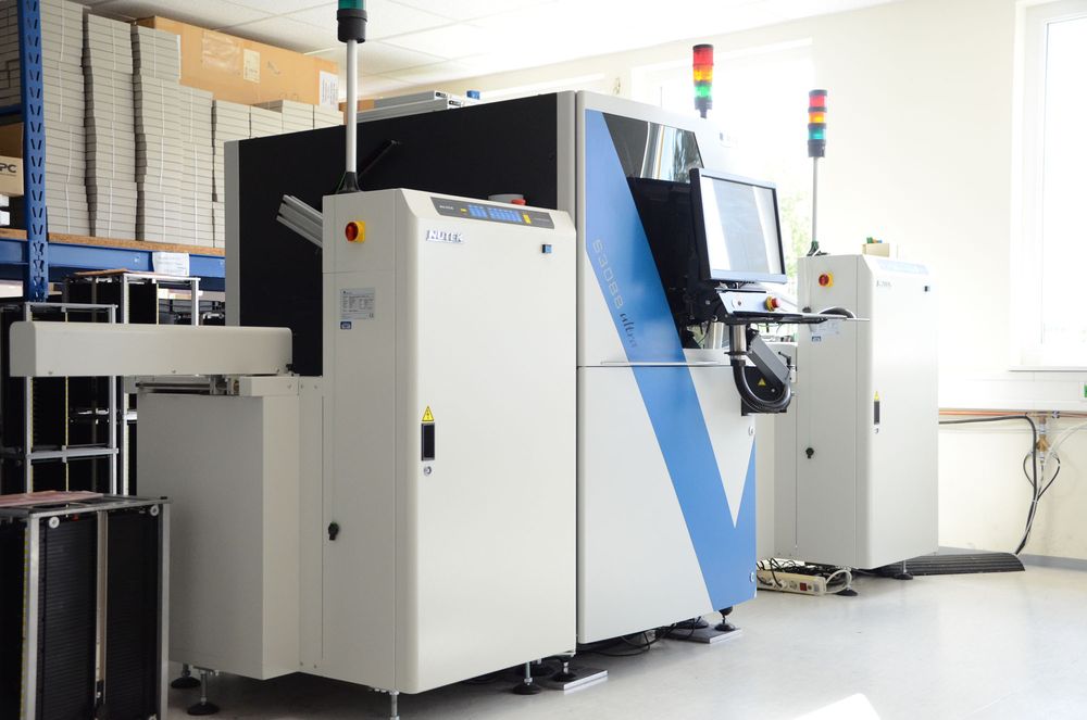
- Viscom AOI S3088 ultra (8 µm resolution)
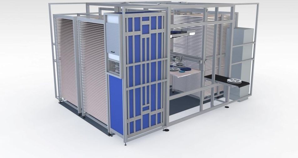
- Fully automated SMD dry storage system KLS
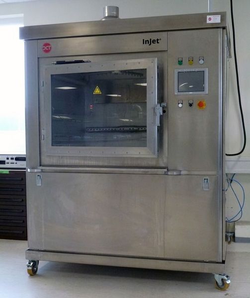
- Solder frame cleaning system
- Ultrasonic cleaning bath
- Hot air oven
- Printed circuit board laser cells
- Nutek inline peripherals
Assemblies and services
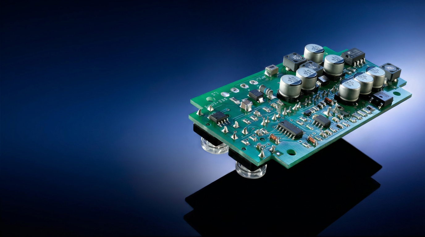
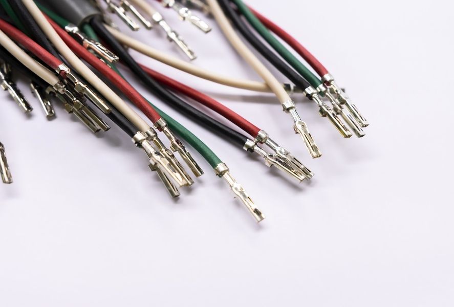
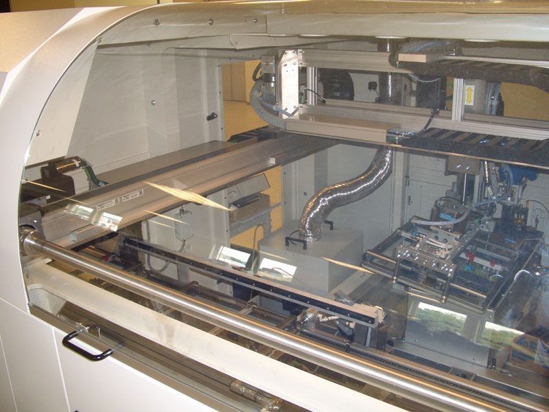
Inside the production
Industries
Processes & technical limits
| Processes | Tolerance | Max. part | Weight | Lot size | Materials |
|---|---|---|---|---|---|
| SMD population (single- and double-sided, 1.5 million components/week)Assembly | – | – | – | Small series – Medium series | Printed circuit boards, SMD/THT components, Fine pitch, BGA |
| Automated snap-in populationAssembly | – | 460 mm × 400 mm | 4.5 kg | – | Snap-in connectors, Electronic components |
| Conventional (THT) population / re-populationAssembly | – | – | – | Very small series | Printed circuit boards, THT components |
| Vapor phase solderingJoining | – | – | – | – | Printed circuit boards, BGA, Fine-pitch components |
| Vapor phase soldering vacuum (gas inclusion reduction)Joining | – | – | – | – | Printed circuit boards |
| Inline vapor phase soldering (up to 6 panels)Joining | – | – | – | – | Printed circuit boards |
| Selective soldering (lead-free, nitrogen)Joining | – | 508 mm × 508 mm | – | – | High-mass printed circuit boards |
| Lead-free wave solderingJoining | – | – | – | – | Printed circuit boards |
| AOI inspection (optical placement inspection, 8 µm resolution)Testing | – | 508 mm × 508 mm | – | – | Printed circuit boards |
| Visual inspection and functional testingTesting | – | – | – | – | Electronic components, Printed circuit boards |
| ReworkAssembly | – | – | – | – | Printed circuit boards |
| Final assembly (installation in housings, packaging)Assembly | – | – | – | – | Electronic assemblies |
| Cable assembly / cable harness manufacturingAssembly | – | – | – | – | Cables |
| Solder frame cleaning / condensate trap cleaningSurface | – | 850 mm × 800 mm | – | – | Solder frames, Condensate traps |
| Washing of printed circuit boards (ultrasonic bath, hot air drying)Surface | – | – | – | – | Printed circuit boards |
| Coating of printed circuit boardsSurface | – | – | – | – | Printed circuit boards |
| Potting (hard resin casting, silicone, wax)Surface | – | – | – | – | Printed circuit boards |
| Electronic development (control technology, power electronics, e²ms)Engineering | – | – | – | – | Printed circuit boards, Power electronics assemblies |
| Component purchasing / material procurementEngineering | – | – | – | – | Electronic components |
| SMD dry storage (IPC-compliant, 40°C, <5% RH)Engineering | – | – | – | – | SMD components, Bare printed circuit boards |
22 Anlagen & Maschinen
| Machine | Manufacturer / model | Quantity | Working area | Year built | Site |
|---|---|---|---|---|---|
| SMD placement machine (chip shooter) | Hanwha SM471plus | 1 | Board size 610x460 mm; components 01005 to 14 mm edge length, max. 12 mm height; 75,000 cph | – | Heßdorf |
| SMD placement machine | Hanwha SM481 | 1 | Board size 460x400 mm; components from 0402 to 55 mm edge length, max. 15 mm height | – | Heßdorf |
| SMD placement machine | Hanwha SM482plus | 1 | Board size 460x400 mm; components from 0201 to 55 mm edge length, max. 15 mm height | – | Heßdorf |
| SMD placement machine for snap-in technology | Hanwha SM485 | 1 | Board size 460x400 mm, max. 4.5 kg; components from 0402 to 21 mm; placement force 0.5–50 N; ±30 µm | – | Heßdorf |
| SMD placement machine (chip shooter) | Samsung SM411 | 1 | Components 0201 to 14x14 mm | – | Heßdorf |
| SMD placement machine | Samsung SM421 | 2 | Placement accuracy ±30 µm; 1x stand-alone | – | Heßdorf |
| Solder paste printer | DEK Horizon 01iX | 1 | – | – | Heßdorf |
| Solder paste printer | DEK Horizon 03iX | 1 | – | – | Heßdorf |
| Solder paste printer | DEK Infinity | 1 | – | – | Heßdorf |
| Vapor phase soldering system | Asscon VP56 | 1 | – | – | Heßdorf |
| Inline vapor phase soldering system | Asscon VP2000 | 1 | up to 6 panels simultaneously | – | Heßdorf |
| Vapor phase soldering system with vacuum phase | Asscon VP6000 | 1 | – | – | Heßdorf |
| AOI system | Viscom S3088 ultra | 1 | Printed circuit boards max. 508 x 508 mm, resolution 8 µm (XM camera module) | – | Heßdorf |
| Inline selective soldering system | Ersa Versaflow (Versaflex soldering module, 2 pots) | 1 | Boards up to 508x508 mm; nozzles min. 3 mm | 2024 | Heßdorf |
| Selective soldering system | Seho | 1 | Printed circuit boards up to 350 x 350 mm; nozzles min. 3 mm | – | Heßdorf |
| Laser cells | – | – | – | – | Heßdorf |
| Lead-free wave soldering system | – | 1 | – | 2008 | Heßdorf |
| SMD dry storage system | KLS | 1 | approx. 5700 180 mm reels, 440 330 mm reels, approx. 230 tray stacks; 40°C, <5% RH | 2013 | Heßdorf |
| Solder frame cleaning system | – | 1 | max. 850 x 800 x 610 mm; up to 6 solder frames simultaneously | – | Heßdorf |
| Ultrasonic cleaning bath | – | 1 | – | – | Heßdorf |
| Hot air oven | – | – | – | – | Heßdorf |
| Nutek peripherals (inline handling) | Nutek | – | – | – | Heßdorf |
Additional services
Quality and certification
All printed circuit boards undergo AOI inspection (Viscom S3088 ultra, 8 µm resolution) as well as visual and functional testing by qualified personnel; defects are assessed and reworked. The company is certified to DIN EN ISO 9001:2015 and has been recognized as an audited UL assembler (Z353, UL 796) since 2019.
| Evidence | Heßdorf |
|---|---|
| ISO 9001 | |
| UL Recognized Component (Z353) |
Company history
- 1980
Founded by Hannelore Birkholz (sources are contradictory: the homepage names Willhelm Birkholz as company founder), population of in-house developed controls for soldering machines, started in a private home on approx. 20 m²
- 1981
Move to the first own production facility in Erlangen-Bruck, up to 10 employees
Move to Erlangen-Eltersdorf due to lack of space with the advent of SMD technology
- 2006
Start of SMD manufacturing in two-shift operation; investments in a second vapor phase soldering machine, fully automatic solder paste printer, AOI system and printed circuit board laser cell
- 2008
Occupancy of the new production building in Heßdorf (01.05.2008), approx. 2,600 m², investment in a lead-free wave soldering system and an additional SMD placement line, doubling of machine placement capacity
- 2010
Renaming to Birkholz Elektronische Geräte GmbH effective 01.01.2010, management under Bernd Birkholz
- 2013
World's first fully automated SMD dry storage system (KLS) commissioned in February 2013
- 2019
Certified as an audited UL assembler since October 2019
- 2024
Acquisition by KRIWAN Holding (Forchtenberg) on 10.01.2024; management under Dr. Christian Ellwein and Thomas Scheidel
- 2024
New ISO-9001 certification valid from 01.07.2024
- 2024
New Ersa inline selective soldering system (Versaflex) since December 2024