Develops Integrated Graphene Photonics (IGP™) for the integration of photonics and electronics on a single wafer.

Black Semiconductor GmbH
Aachen (DE) · Netherlands (Applied Nanolayers)New on Amplifa
About Black Semiconductor
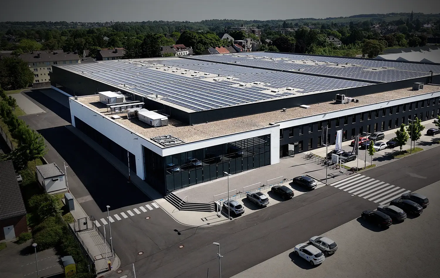
Black Semiconductor is a semiconductor company founded in Aachen in 2020 that develops the integration of photonics and electronics on the same wafer. At its core is the proprietary IGP™ technology (Integrated Graphene Photonics): wafer-scale, single-crystal graphene is produced by CVD with epitaxial growth on an engineered substrate and integrated into chips using CMOS-compatible processes (BEOL). Based on this, graphene-based photodetectors (photo-thermoelectric and bolometric, bandwidth over 500 GHz), modulators and electronic-photonic chips (EPIC) are created. In addition, the company develops glass panel interposers with optical waveguides. Customer industries are the semiconductor industry as well as datacenters and high-performance computing (HPC, AI) with chip-to-chip communication. The FabONE headquarters in Aachen comprises 15,000 m² of production and 2,000 m² of office space; a scalable pilot line for 300-mm wafer technology is being built there. In 2025, Black Semiconductor acquired the Dutch graphene specialist Applied Nanolayers with an industrial 200-mm wafer platform for volume production of graphene.
- Site
- Aachen
- Processes
- CVD growth of single-crystal graphene (epitaxial growth on engineered substrate), Wafer-scale transfer and integration of single-layer graphene onto wafers (high-temperature, Graphene-based photodetectors (photo-thermoelectric effect, bolometric, bandwidth >500, Graphene modulators (two graphene layers with insulator, light modulation via Pauli blocking), Integrated Graphene Photonics™ (IGP) – CMOS-compatible integration of photonics and electronics on, Glass Panel Interposer – electrical connections with dense optical waveguides, Wafer-scale single-crystal graphene production (CVD, epitaxial growth), Integrated Graphene Photonics (IGP™): photodetectors and modulators on chip wafers
- Materials
- Graphene (single-crystal, wafer-scale), Glass (Glass Panel Interposer), Single-Crystal Graphene (wafer-scale), Integrated Graphene Photonics™, Electronic-Photonic Chip (EPIC)
- Founded
- 2020
- Industries
- Semiconductor industry, Datacenter / High-Performance Computing (HPC, AI), Chip-to-Chip Communication / Interconnects
- 01
CVD growth of single-crystal graphene (epitaxial, engineered substrate)
- 02
Wafer-scale transfer and integration onto wafers
- 03
Interface engineering, dielectric capping, CMOS-compatible contact formation
- 04
Device integration: photodetectors, modulators, EPIC
- 05
Characterization & device validation
Materials & Processes
Single-Crystal Graphene (wafer-scale)
Single-crystal, low-defect graphene produced by chemical vapor deposition with epitaxial growth for high-speed and energy-efficient semiconductor devices.
Integrated Graphene Photonics™
CMOS-compatible integration of graphene photonics and electronics on a single wafer (BEOL), including on 5nm/3nm CMOS nodes.
Glass (Glass Panel Interposer)
Glass panel interposer with dense optical waveguides for electrical connections and optical chip-to-chip communication.
Electronic-Photonic Chip (EPIC)
Integration of electronic IC and photonic IC on a single wafer for chip-to-chip optical interconnects.
Sites
Aachen (FabONE)
DEHeadquarters, production & administration; pilot line for 300-mm wafer technology (construction start 2026)
- Materials
- Graphene, silicon, glass
- Scalable pilot line for 300-mm wafer technology
Netherlands (Applied Nanolayers)
NLGraphene production on an industrial 200-mm wafer platform (acquisition March 2025)
- Materials
- Graphene
- Industrial 200-mm wafer platform for graphene production
Components & Products
Inside the production


Industries
Processes & technical limits
| Processes | Tolerance | Max. part | Weight | Lot size | Materials |
|---|---|---|---|---|---|
| CVD growth of single-crystal graphene (epitaxial growth on engineered substrate)Semiconductor manufacturing | – | 300 mm wafer (pilot line) | – | – | Graphene, Carbon |
| Wafer-scale transfer and integration of single-layer graphene onto wafers (high-temperatureSemiconductor manufacturing | – | – | – | – | Graphene |
| Graphene-based photodetectors (photo-thermoelectric effect, bolometric, bandwidth >500Semiconductor manufacturing | – | – | – | – | Graphene |
| Graphene modulators (two graphene layers with insulator, light modulation via Pauli blocking)Semiconductor manufacturing | – | – | – | – | Graphene |
| Integrated Graphene Photonics™ (IGP) – CMOS-compatible integration of photonics and electronics onSemiconductor manufacturing | – | 300 mm wafer | – | – | Graphene, Silicon |
| Glass Panel Interposer – electrical connections with dense optical waveguidesSemiconductor manufacturing | – | – | – | – | Glass |
2 Anlagen & Maschinen
| Machine | Manufacturer / model | Quantity | Working area | Year built | Site |
|---|---|---|---|---|---|
| Pilot line for 300-mm wafer technology (FabONE) | – | – | 15,000 m² production area, 2,000 m² office | 2025 (Baub | Aachen |
| Industrial 200-mm wafer platform for graphene production (acquired from Applied Nanolayers) | Applied Nanolayers | – | – | 2025 (Akqu | Netherlands |
Additional services
History
- 2020–22
Official founding by Daniel and Sebastian Schall; €11.2 million VC financing including public funding, co-led by Vsquared and Cambium.
- 2023
Start of building a wafer manufacturing technology.
- 2024
€228.7 million IPCEI grant and €25.7 million private investment secured.
- 2025
Move into the FabONE facility (15,000 m² production, 2,000 m² office); construction start of the scalable pilot line for 300-mm wafer technology; acquisition of Applied Nanolayers (NL); SPARK Award 2025; finalist of the German Founders' Award.
- 2025-11-19
Exyte signs the construction contract for the FabONE facility.
- 2026
Further fab expansion and next financing phase; FabONE construction start in March 2026.