Fabless design house for custom RF and mixed-signal ASICs from specification to qualified delivery.

Bruco Integrated Circuits B.V.
Borne (HQ), Netherlands · Nijmegen, Netherlands · Berlin, GermanyNew on Amplifa
About Bruco IC
Bruco IC is an independent fabless IC design house headquartered in Borne (Netherlands) with additional offices in Nijmegen and Berlin. The company develops custom RF, analog and mixed-signal ASICs for applications where standard ICs do not meet the requirements, taking on the entire process from system architecture through tape-out to qualified silicon delivery, including supply chain management. Development is carried out in technologies such as CMOS, BiCMOS, SiGe, (RF-)SOI, BCD, FD-SOI as well as GaN and LDMOS for power ranges of 1 W to 1000 W in RF power amplifiers (Doherty architectures). For validation, Bruco IC operates its own RF measurement and test laboratory in Borne with vector-receiver load-pull and S-parameter measurements up to 18 GHz, as well as a mechanical laboratory for prototypes (baseplates, inserts). Qualification is performed in accordance with JEDEC JESD47 and AEC-Q100. Customers come from industries such as telecommunication/satcom, 5G base stations, GNSS/autonomous systems, automotive, industrial, defense and next-generation computing (photonics, quantum computing, AI). The team comprises more than 35 IC design and application engineers with Bachelor's, Master's and PhD degrees.
- Site
- CS Borne
- Processes
- Turnkey ASIC development (feasibility to supply), Custom RF IC design (DC to mmWave, 30 GHz), Custom mixed-signal IC design (ADC, DAC, signal processing), Doherty power amplifier (DPA) ASIC design 1W–1000W, 100–380 MHz, RF engineering support / staff augmentation, 3D EM modelling, Load-pull measurement (harmonic, fundamental), S-parameter measurements (0.1–18 GHz, CW/pulsed)
- Materials
- CMOS, BiCMOS, SiGe, SOI / RF-SOI, FD-SOI, BCD, GaN (gallium nitride), LDMOS
- Certificates
- JEDEC JESD47 qualification, AEC-Q100 qualification
- Founded
- 1989
- Employees
- 35+ (IC design and
- Industries
- Telecommunications/satcom, 5G base stations, Radar, GNSS/positioning & autonomous systems, Drones & precision agriculture, Automotive
- 01
Feasibility & architecture study
- 02
Circuit design & verification
- 03
Test development & silicon characterization
- 04
Qualification (JEDEC JESD47 / AEC-Q100)
- 05
Tape-out via foundry partners
- 06
OSAT assembly & production testing
- 07
Supply chain & lifecycle management
Technologies & Processes
CMOS
Baseline technology for mixed-signal ASICs such as ADCs, DACs and signal processing.
BiCMOS
Used for high-performance RF ICs from sub-6 GHz to mmWave.
SiGe
Typical technology for high-frequency RF designs up to 30 GHz.
SOI / RF-SOI
For front-end RF ICs such as LNAs, switches and integrated receivers.
FD-SOI
Process option in the turnkey ASIC portfolio for specific performance targets.
BCD
Technology for gate drivers and power applications.
GaN (gallium nitride)
For highest power density and efficiency, e.g. in 5G base stations, radar and satcom.
LDMOS
Proven technology for RF power amplifiers from 0.1 to 4 GHz.
Locations
Borne
NLHeadquarters: design, RF laboratory, mechanical laboratory
- Materials
- CMOS, BiCMOS, SiGe, SOI, GaN, LDMOS
- Vector-receiver load-pull measurement system (harmonic 0.6–9.0 GHz, fundamental 0.6–18.0 GHz, DUT max. 50 W CW / 500 W pulsed)
- 2× Maury harmonic tuner (0.6–18.0 GHz)
- 2× Maury low-loss coupler (0.1–18.0 GHz)
- Rohde & Schwarz vector network analyzer (26 GHz)
- Keysight power supplies / Keithley multimeters
- Anteverta universal test fixture
- IVCAD software (Dassault Systèmes)
- Custom test fixtures for SMT and leaded devices
- Mechanical laboratory for baseplates & inserts
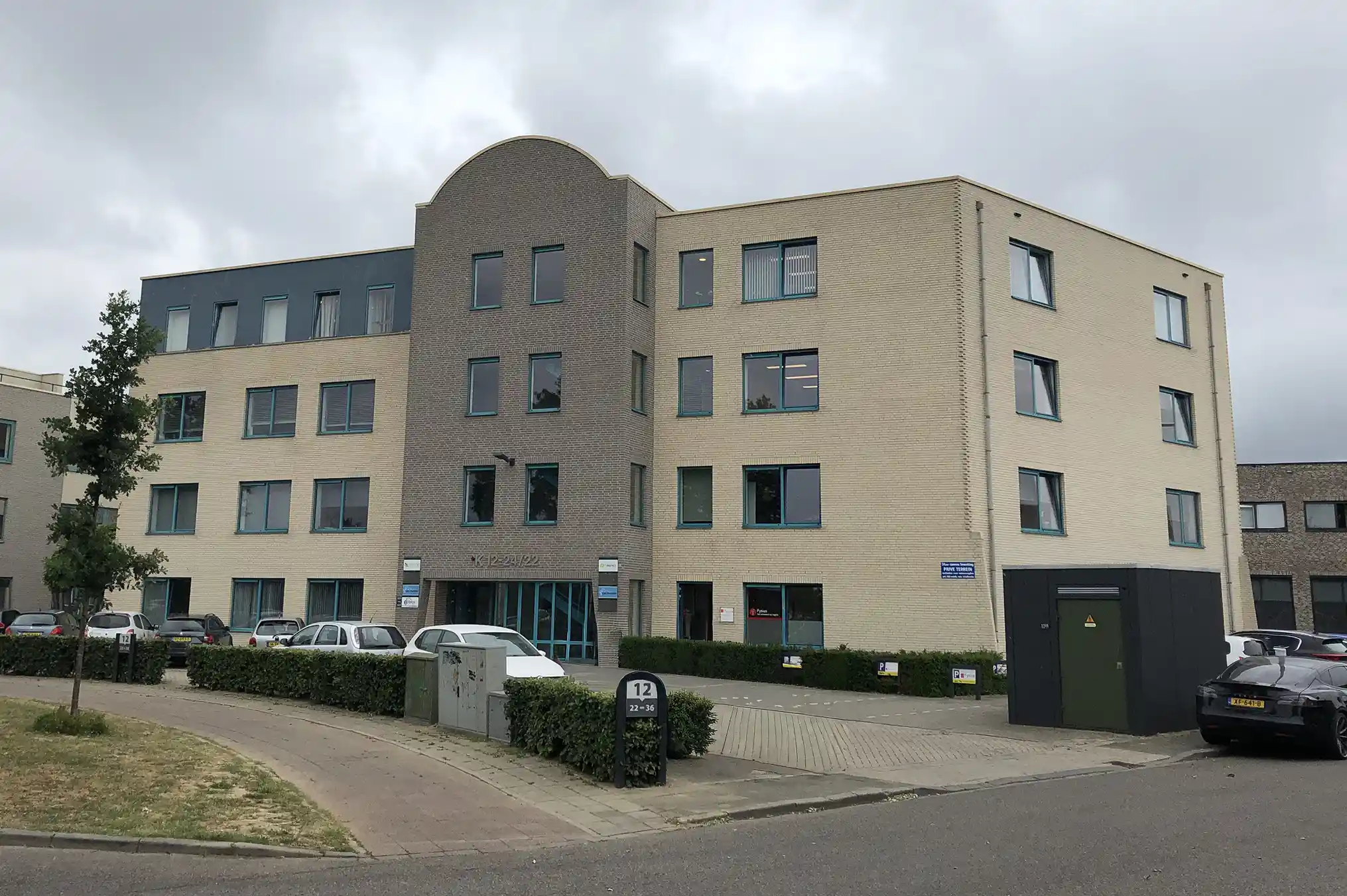
Nijmegen
NLOffice / engineering
Berlin
DEOffice / engineering
IC Solutions & Services
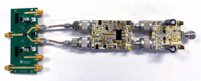
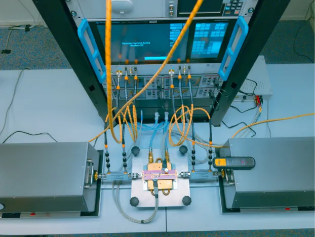
Inside the production
Industries
Processes & technical limits
| Processes | Tolerance | Max. part | Weight | Lot size | Materials |
|---|---|---|---|---|---|
| Turnkey ASIC development (feasibility to supply)Engineering | – | – | – | – | CMOS, BiCMOS, SiGe, SOI, BCD, FD-SOI, GaN |
| Custom RF IC design (DC to mmWave, 30 GHz)Engineering | – | – | – | – | CMOS, BiCMOS, SiGe, RF-SOI, GaN |
| Custom mixed-signal IC design (ADC, DAC, signal processing)Engineering | – | – | – | – | CMOS |
| Doherty power amplifier (DPA) ASIC design 1W–1000W, 100–380 MHzEngineering | – | – | 1 W – 1000 W | – | GaN, LDMOS |
| RF engineering support / staff augmentationEngineering | – | – | – | – | – |
| 3D EM modellingEngineering | – | – | – | – | – |
| Load-pull measurement (harmonic, fundamental)Testing | – | – | – | – | GaN, LDMOS |
| S-parameter measurements (0.1–18 GHz, CW/pulsed)Testing | – | – | – | – | GaN, LDMOS |
| Qualification in accordance with JEDEC JESD47 / AEC-Q100 (cold climate, thermal cycling, humidityTesting | – | – | – | – | – |
| Supply chain management (foundry, OSAT, production testing, lifecycle)Assembly | – | – | – | – | – |
| Mechanical prototyping (manufacturing and soldering of baseplates and inserts)Assembly | – | – | – | – | – |
9 Anlagen & Maschinen
| Machine | Manufacturer / model | Quantity | Working area | Year built | Site |
|---|---|---|---|---|---|
| Vector-receiver load-pull measurement system | Maury / Rohde & Schwarz / Keysight | 1 | Harmonic 0.6–9.0 GHz, fundamental 0.6–18.0 GHz, DUT max. 50 W CW / 500 W pulsed | – | Borne, NL |
| Maury harmonic tuner | Maury | 2 | 0.6–18.0 GHz | – | Borne, NL |
| Maury low-loss coupler | Maury | 2 | 0.1–18.0 GHz | – | Borne, NL |
| Vector network analyzer (26 GHz) | Rohde & Schwarz | 1 | 26 GHz | – | Borne, NL |
| Power supplies / multimeters | Keysight / Keithley | – | – | – | Borne, NL |
| Universal test fixture for leaded devices | Anteverta IVCAD (Dassault Systèmes software) | 1 | – | – | Borne, NL |
| Custom test fixtures for SMT and leaded devices | – | – | – | – | Borne, NL |
| In-house RF measurement and test laboratory | – | 1 | 0.7–4 GHz tuning/characterization | – | Borne, NL |
| In-house mechanical laboratory (manufacturing/soldering of baseplates & inserts) | – | 1 | – | – | Borne, NL |
Additional services
Reference customers
Quality & Qualification
Verification and qualification are performed according to standardized procedures in accordance with JEDEC JESD47 (industrial) and AEC-Q100 (automotive), including accelerated aging, thermal cycling, humidity and electrical tests. Load-pull and S-parameter measurements (CW and pulsed) for characterization are carried out in the company's own RF laboratory in Borne.
| Evidence | Borne |
|---|---|
| JEDEC JESD47 qualification | |
| AEC-Q100 qualification |
History
- 1989
Company founded.
More than 35 years of experience in turnkey ASIC design; over 100 completed Doherty PA designs and more than 2 million delivered IC solutions.