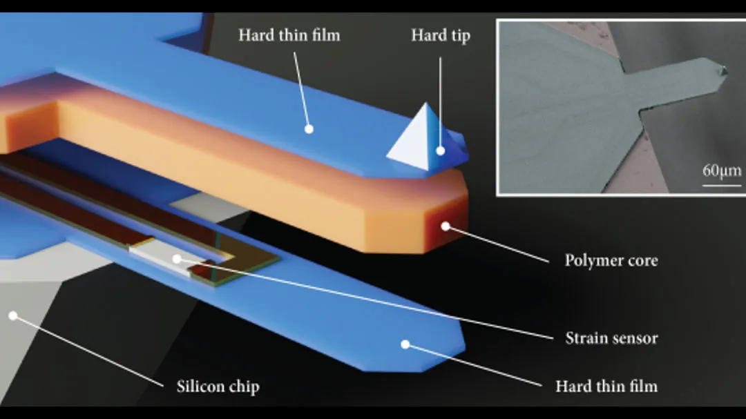
Development of piezoresistive self-sensing cantilevers and readout electronics for laser-free AFM measurements

c-sense GmbH
Langenlois · Wiener Neustadt · ViennaNew on Amplifa
About c-sense
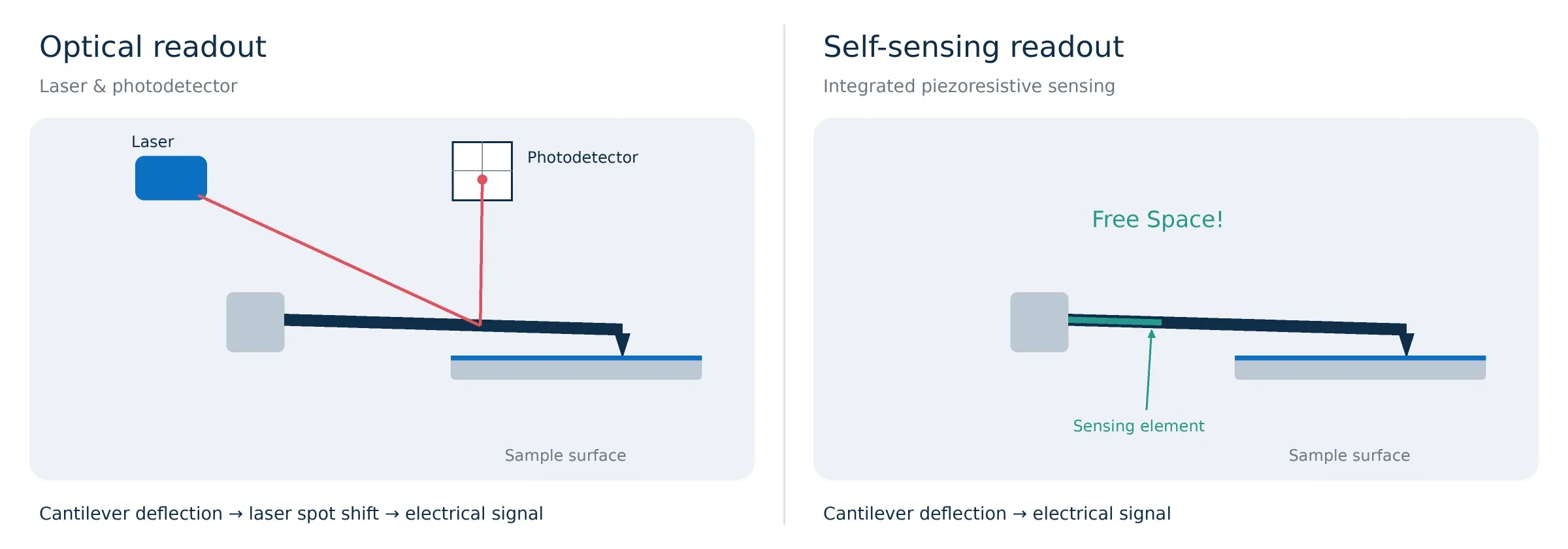
c-sense GmbH is an Austrian nanotechnology company based in Langenlois (Lower Austria) that develops and markets active, self-measuring AFM cantilevers based on piezoresistive sensor technology. By directly integrating the measuring function into the cantilever, optical laser readout is eliminated, making measurements possible in environments where conventional optical beam deflection reaches its limits – for example in cryogenic systems, in vacuum, in SEM systems, in turbid or conductive liquids, and in compact custom research setups. The portfolio includes silicon self-sensing cantilevers with Si tip or tipless, patented trilayer cantilevers (polymer–semiconductor–ceramic thin-film architecture), conductive trilayer cantilevers for KPFM, EFM and cAFM, Quantum Cryogenic Trilayer (QCT) cantilevers, as well as the NanoOne and NanoLab Pro readout electronics. In addition, the company offers Custom Cantilever Development, OEM integration, Application Engineering, AFM Integration, as well as customer support and training. The technology builds on two decades of development as the successor to the SCL Sensor.Tech activities and serves industries such as biotechnology, semiconductor metrology, nanomechanics, quantum technologies and magnetic measurements.
- Site
- Langenlois
- Processes
- Development and distribution of piezoresistive, self-measuring AFM cantilevers (active, self-sensing, Silicon self-sensing cantilevers with integrated electrical readout (with Si tip or, Advanced Trilayer Self-Sensing Cantilevers (patented polymer thin-film trilayer architecture,, Conductive Trilayer Cantilevers for electrical and electrostatic AFM applications (KPFM, EFM,, Quantum Cryogenic Trilayer (QCT) cantilevers for low-temperature and cryogenic research, NanoOne Starter Kit – readout electronics, cables and self-sensing cantilevers as an entry-level, NanoLab Pro electronics (readout electronics), Custom Cantilever Development / made-to-spec custom solutions (custom cantilevers,
- Materials
- Silicon, Polymer (trilayer architecture), Semiconductor thin film (trilayer), Ceramic (trilayer, according to the publication 'polymer–semiconductor–ceramic cantilever'), Polymer–semiconductor–ceramic trilayer, Ceramic (trilayer)
- Certificates
- ISO 9001
- Industries
- Biotechnology, Semiconductor metrology, Nanomechanics, Quantum technologies, Magnetic measurements, Advanced OEM instrumentation
- 01
Product definition
- 02
Cantilever design and sensor development
- 03
Custom Probe / Cantilever Development (with specialized manufacturing partners)
- 04
Readout electronics (NanoOne, NanoLab Pro)
- 05
System and AFM integration
- 06
Application Engineering
- 07
Customer support and training
Materials & Processes
Silicon
Piezoresistive silicon cantilevers with integrated electrical readout, with Si tip or tipless, in various resonance frequencies and stiffnesses.
Polymer–semiconductor–ceramic trilayer
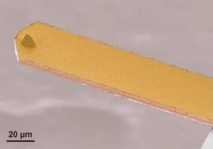
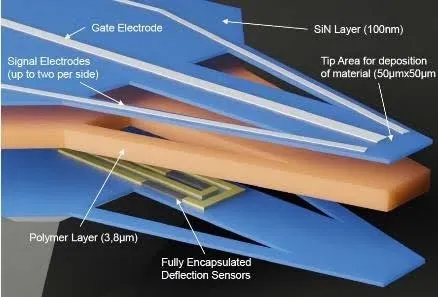
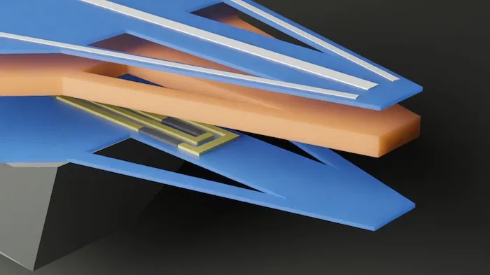
Patented trilayer architecture for high force sensitivity and fast imaging, as published in Nature Electronics.
Semiconductor thin film (trilayer)
Thin-film component of the trilayer cantilevers for self-sensing piezoresistive readout.
Ceramic (trilayer)
Hard layer and tip component of the trilayer cantilevers according to the publication 'polymer–semiconductor–ceramic cantilever'.
Locations
Langenlois
ATHeadquarters
- Materials
- Silicon, trilayer (polymer, semiconductor thin film, ceramic)
- Development and design of self-sensing cantilevers
- Readout electronics
Wiener Neustadt
ATLaboratory (TFZ Technology and Research Center, Viktor Kaplan-Straße 2, Building E – 2nd floor)
- AFM measurement technology
- Application laboratory
Vienna
ATLaboratory (Tech Park Vienna, Gutheil-Schoder-Gasse 17)
Products & Components
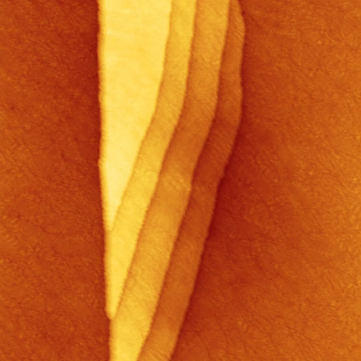
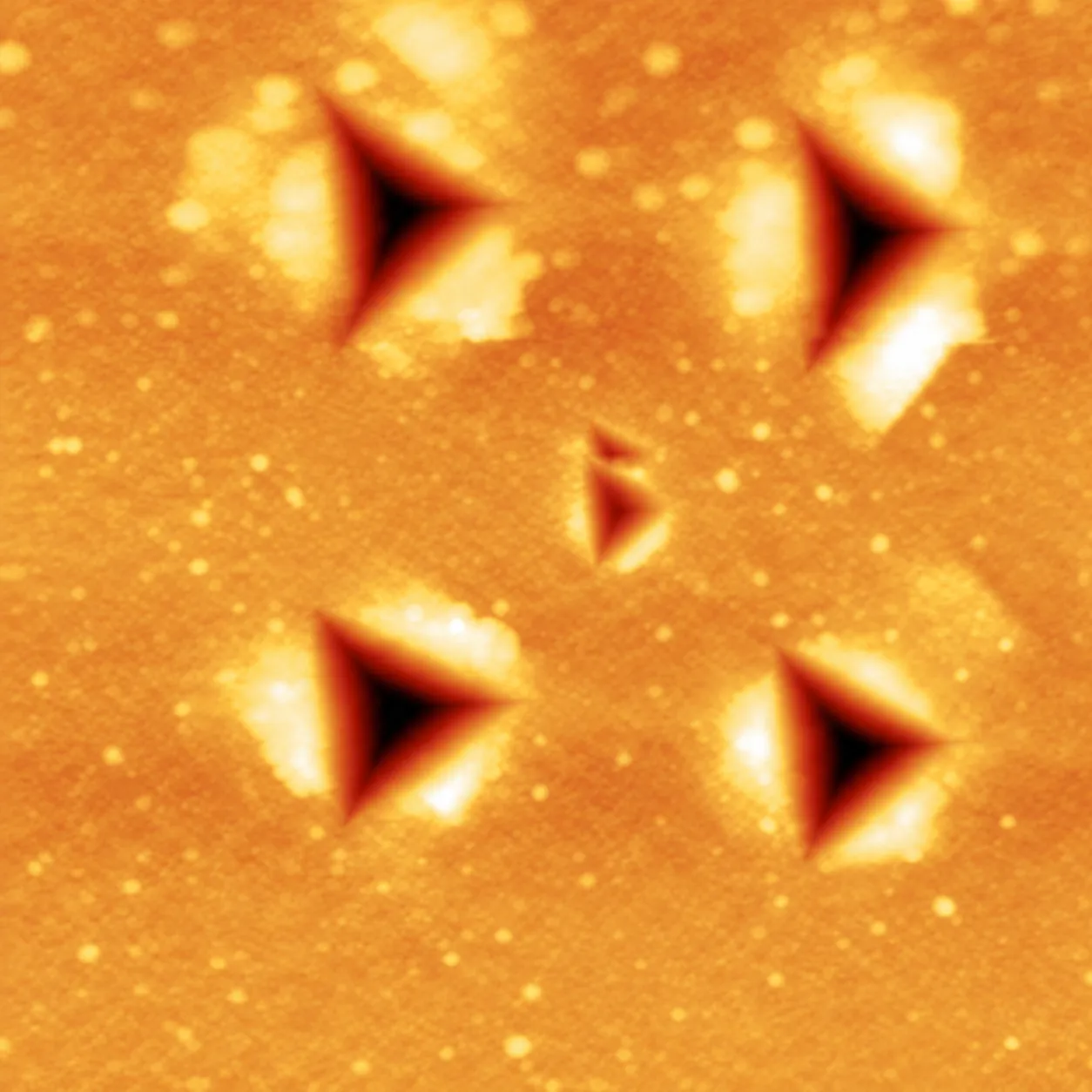
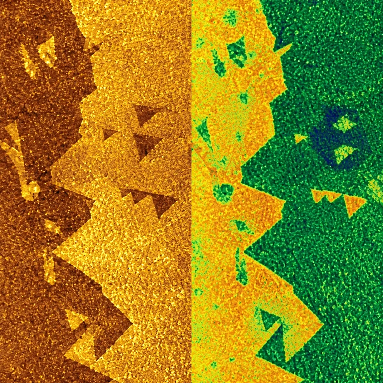
Inside the production
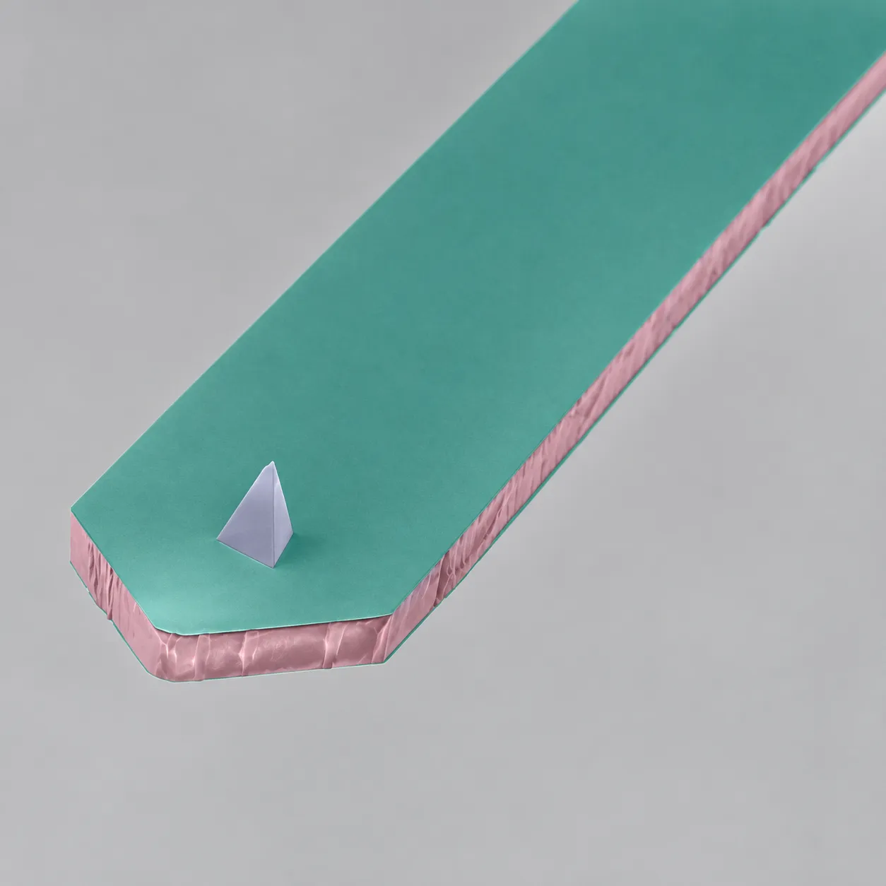
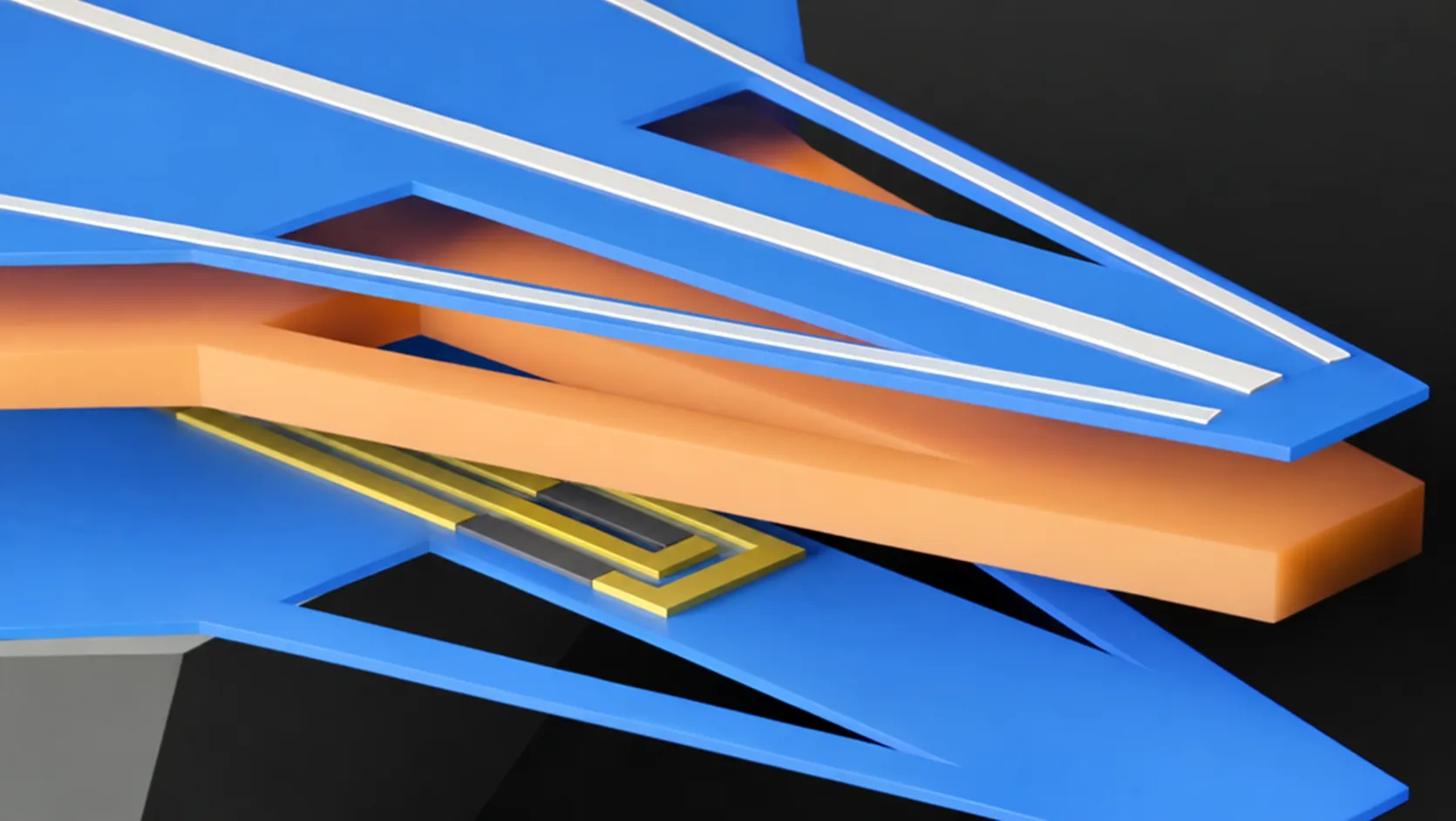
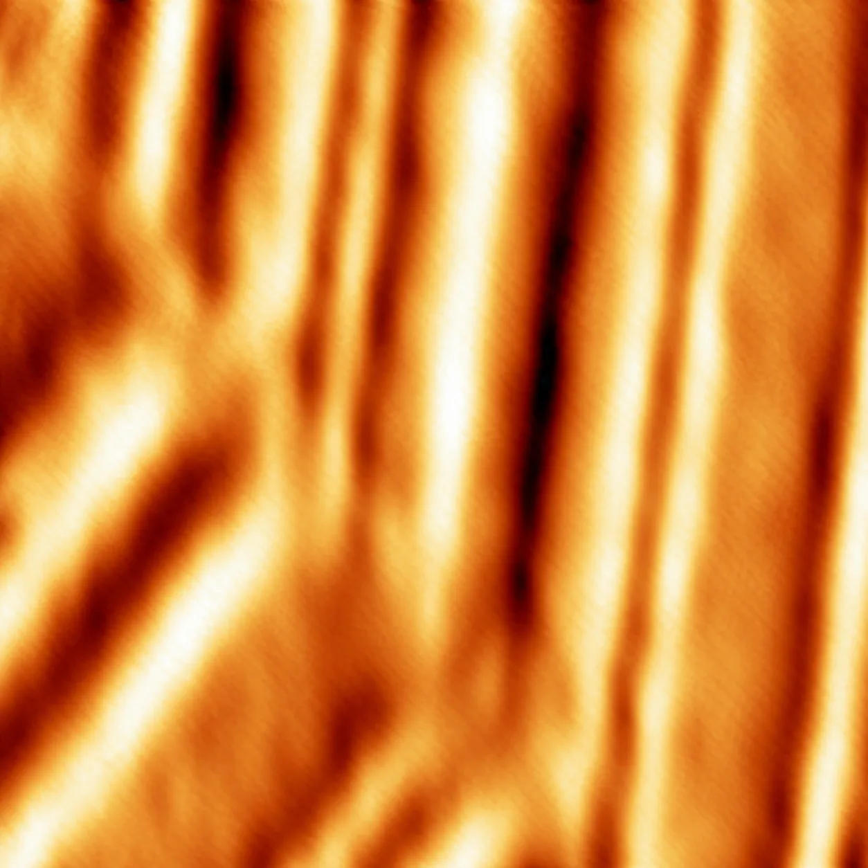
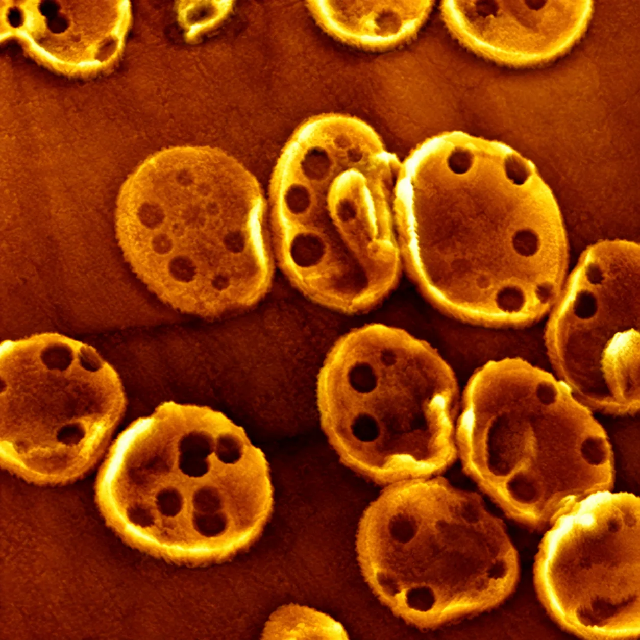
Industries
Processes & technical limits
| Processes | Tolerance | Max. part | Weight | Lot size | Materials |
|---|---|---|---|---|---|
| Development and distribution of piezoresistive, self-measuring AFM cantilevers (active, self-sensingEngineering | – | – | – | – | Silicon, Polymer thin-film trilayer |
| Silicon self-sensing cantilevers with integrated electrical readout (with Si tip orEngineering | – | – | – | – | Silicon |
| Advanced Trilayer Self-Sensing Cantilevers (patented polymer thin-film trilayer architecture,Engineering | – | – | – | – | Polymer, Thin-film semiconductor, Ceramic |
| Conductive Trilayer Cantilevers for electrical and electrostatic AFM applications (KPFM, EFM,Engineering | – | – | – | – | Polymer, Thin-film semiconductor, Ceramic |
| Quantum Cryogenic Trilayer (QCT) cantilevers for low-temperature and cryogenic researchEngineering | – | – | – | – | Polymer, Thin-film semiconductor, Ceramic |
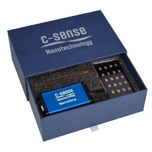
| NanoOne Starter Kit – readout electronics, cables and self-sensing cantilevers as an entry-levelEngineering | – | – | – | – | – |
| NanoLab Pro electronics (readout electronics)Engineering | – | – | – | – | – |
| Custom Cantilever Development / made-to-spec custom solutions (custom cantilevers,Engineering | – | – | – | – | Silicon, Polymer, Thin-film semiconductor, Ceramic |
| AFM measurement technology: topography and structure (surface height, 3D profile, phase imaging)Testing | – | – | – | – | – |
| AFM measurement technology: mechanical properties (stiffness, adhesion, friction, viscoelasticity)Testing | – | – | – | – | – |
| AFM measurement technology: KPFM and EFM (surface potential, work function, doping)Testing | – | – | – | – | – |
| AFM measurement technology: conductive measurements (cAFM, nanoprobing, IV spectroscopy, SSRM)Testing | – | – | – | – | – |
| AFM measurement technology: low-temperature and quantum measurements (Quantum Twisting Microscopy)Testing | – | – | – | – | – |
| AFM measurement technology: MFM (magnetic force microscopy)Testing | – | – | – | – | – |
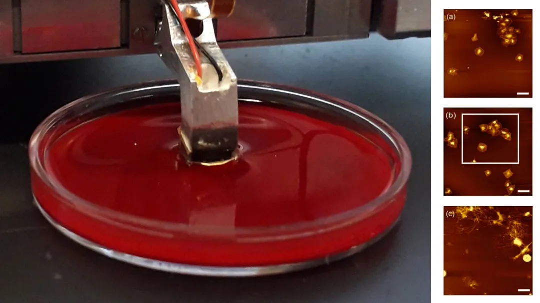
| AFM measurement technology: in-liquid and biosensing (opaque and transparent liquid environments)Testing | – | – | – | – | – |
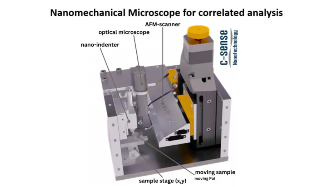
| Nanomechanical microscope for correlated analysis / CAS-C NanoInspect for correlatedTesting | – | – | – | – | – |
| System integration, OEM development, Application Engineering and electronics for high-performanceEngineering | – | – | – | – | – |
Additional services
Reference customers
Quality & Standards
c-sense ensures quality through Application Engineering, custom sensor development and direct support by application scientists; the technology is backed by peer-reviewed publications (including Nature Electronics).
| Evidence | Langenlois |
|---|---|
| ISO 9001 |
History
Continuation of the SCL Sensor.Tech activities; the technology is based on two decades of self-sensing cantilever development