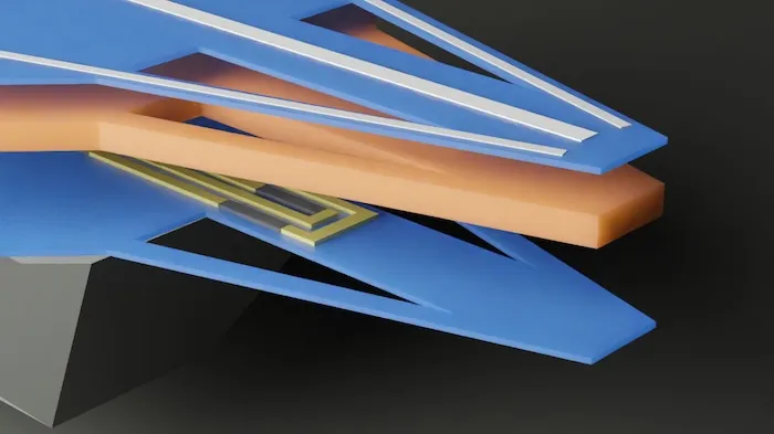
Development and marketing of piezoresistive self-sensing cantilevers for laser-free AFM measurements at the nanoscale.

c-sense GmbH
Langenlois (headquarters) · Wiener Neustadt (TFZ laboratory) · Vienna (Tech Park Vienna laboratory)New on Amplifa
About c-sense
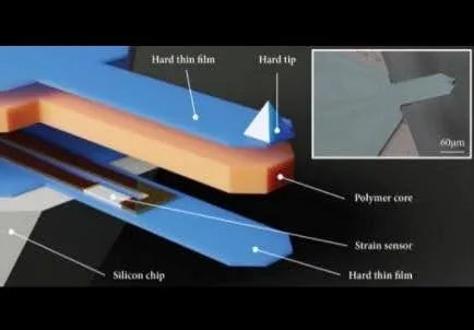
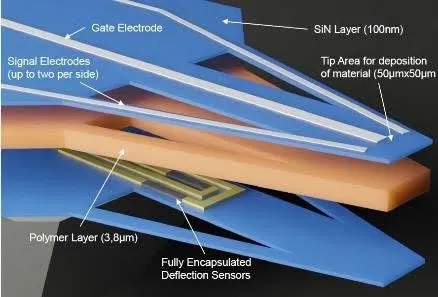
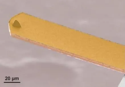
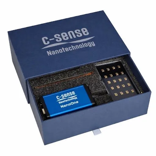
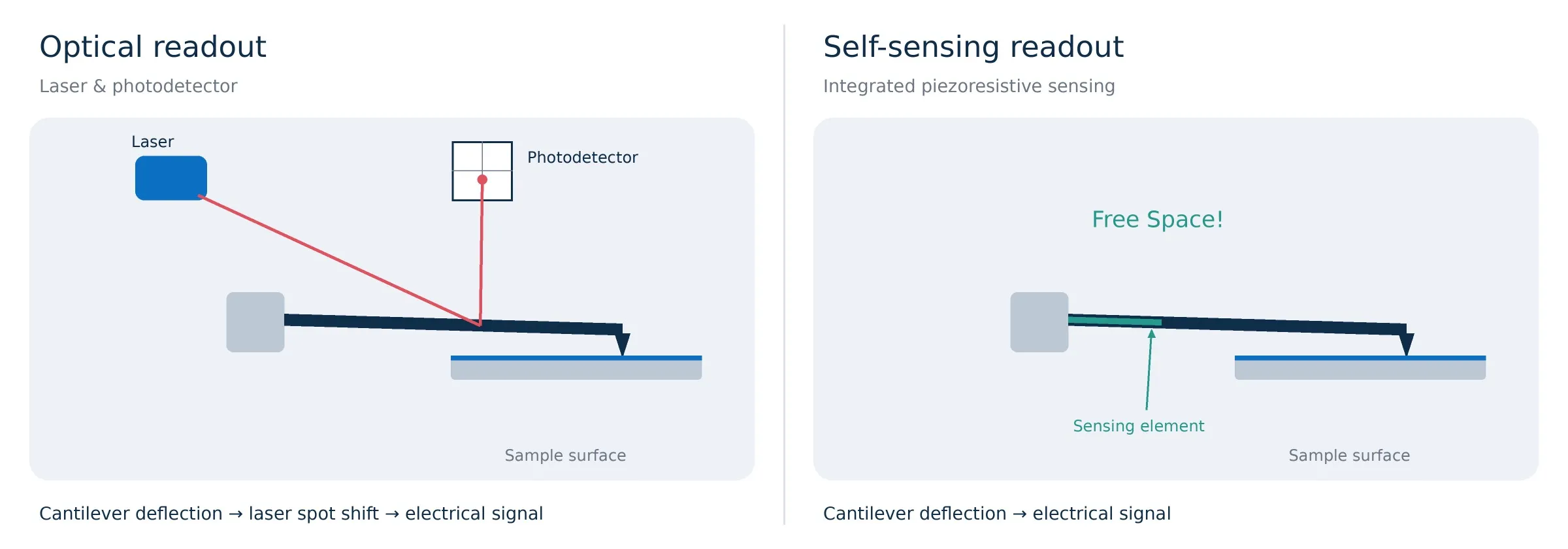
c-sense GmbH is an Austrian nanotechnology company headquartered in Langenlois (Lower Austria), with laboratories at the TFZ Wiener Neustadt and in the Tech Park Vienna. The company develops and markets piezoresistive self-sensing cantilevers for atomic force microscopy (AFM), in which detection of the cantilever deflection is electrically integrated – without external laser alignment and an optical detection path. The product portfolio comprises silicon cantilevers with and without tips, patented trilayer cantilevers based on a polymer thin-film architecture, conductive variants for KPFM, EFM and cAFM as well as Quantum Cryogenic Trilayer (QCT) cantilevers for cryogenic and quantum measurements. In addition, c-sense offers readout electronics (NanoOne Starter Kit, NanoLab Pro), custom cantilever development, OEM integration and application engineering. The technology, which is based on decades of development of piezoresistive self-sensing cantilevers and continues the activities of SCL Sensor.Tech, has been published in Nature Electronics. Customers include universities, research institutions and industrial partners in Europe, North America and Asia, particularly from biotechnology, semiconductor metrology, nanomechanics, quantum technologies and magnetic measurements.
- Site
- Langenlois
- Processes
- Manufacture of piezoresistive self-sensing AFM cantilevers (MEMS microfabrication), Development and customization of cantilever solutions (custom development, OEM integration), System integration of sensor technology and readout electronics (NanoOne, NanoLab Pro), Nanoscale measurement services: topography, mechanical properties, KPFM/EFM, cAFM, MFM, bio-AFM, Custom Cantilever Development, OEM Integration, AFM Integration, Application Engineering
- Materials
- Silicon, Polymer thin film (trilayer architecture), Semiconductor thin film (trilayer), Ceramic thin film (trilayer), Trilayer architecture (polymer thin film)
- Industries
- Biotechnology, Semiconductor metrology, Nanomechanics, Quantum technologies, Magnetic measurements, OEM instrumentation
- 01
Product definition and custom cantilever development
- 02
MEMS microfabrication with specialized manufacturing partners
- 03
Electronics for high-performance readout (NanoOne, NanoLab Pro)
- 04
System integration and AFM integration
- 05
Application engineering, customer support and training
Materials & Processes
Silicon
Base material of the piezoresistive self-sensing cantilevers, with or without silicon tip, in various resonance frequencies and stiffnesses.
Trilayer architecture (polymer thin film)
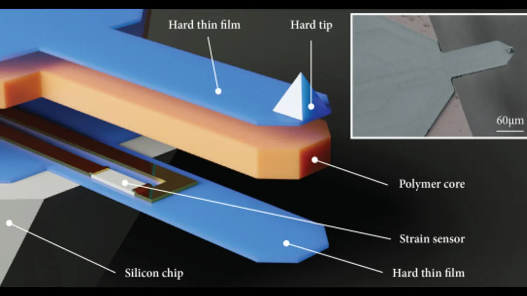
Patented polymer–semiconductor–ceramic layer structure for high force sensitivity and liquid-compatible MEMS applications.
Semiconductor thin film (trilayer)
Used as a layer in the trilayer cantilevers for conductive and electrostatic AFM measurements.
Ceramic thin film (trilayer)
Hard thin film in the trilayer structure, optimized for cryogenic and quantum measurement environments.
Sites
Langenlois
ATHeadquarters
- Materials
- Silicon, trilayer
Wiener Neustadt
ATLaboratory at the TFZ Technology and Research Centre, Viktor Kaplan-Straße 2, Building E – 2nd floor
- NanoOne
- NanoLab Pro
Vienna
ATLaboratory at the Tech Park Vienna, Gutheil-Schoder-Gasse 17
Components & Products
Inside the production
Industries
Processes & technical limits
| Processes | Tolerance | Max. part | Weight | Lot size | Materials |
|---|---|---|---|---|---|
| Manufacture of piezoresistive self-sensing AFM cantilevers (MEMS microfabrication)Engineering | – | – | – | – | Silicon, Polymer thin-film trilayer, Semiconductor thin film, Ceramic thin film |
| Development and customization of cantilever solutions (custom development, OEM integration)Engineering | – | – | – | – | – |
| System integration of sensor technology and readout electronics (NanoOne, NanoLab Pro)Assembly | – | – | – | – | – |
| Nanoscale measurement services: topography, mechanical properties, KPFM/EFM, cAFM, MFM, bio-AFMTesting | – | – | – | – | – |
1 Anlagen & Maschinen
| Machine | Manufacturer / model | Quantity | Working area | Year built | Site |
|---|---|---|---|---|---|
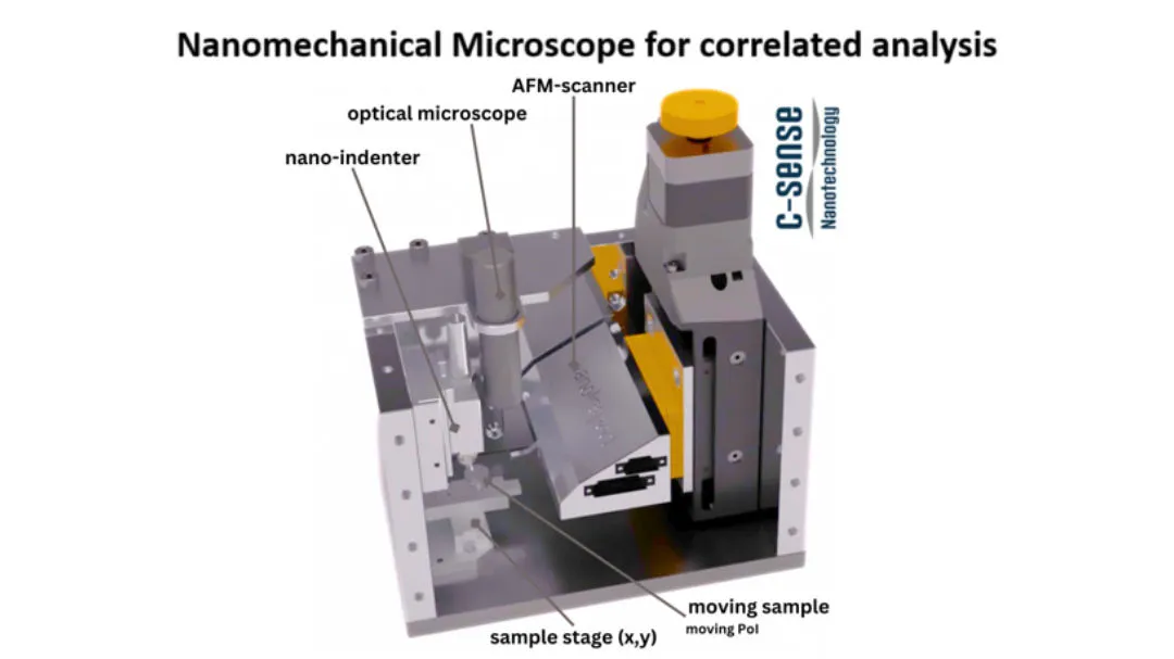
| AFM metrology / nanomechanical microscope | c-sense NanoOne Starter Kit / NanoLab Pro electronics | – | – | – | Wiener Neustadt / Langenlois / Vienna |
Additional services
Reference customers
History
Originated from the continuation of the SCL Sensor.Tech activities: The technology is based on decades of development of piezoresistive self-sensing cantilevers.
Eureka label for the CAS-C project NanoInspect with the partners Alemnis, Danube University Krems and EPFL.
- 2024
Publication of the trilayer technology in Nature Electronics (N. Hosseini et al., DOI 10.1038/s41928-024-01195-z).