
Inspection and Metrology Systems for Semiconductor Manufacturing – from Front-End to Post Dicing

Camtek Ltd.
Migdal Ha'emek (HQ, IL) · Kirchheim near Munich · Bergisch Gladbach · Beaverton, OR · Hong Kong · Suzhou · Hsinchu City · Suwon-si · Tokyo · SingaporeNew on Amplifa
About Camtek
Camtek is a developer and manufacturer of inspection and metrology systems for the semiconductor industry. The systems inspect and measure wafers throughout the entire production process – from front-end through mid-end manufacturing to post-dicing inspection – ensuring that only defect-free chips (Known Good Die) end up in final products. The portfolio includes the Eagle platform for 2D and 3D inspection with sub-micron accuracy (CLIP light interferometry) as well as the Golden Eagle for panel inspection up to 650 mm × 650 mm in Fan-Out Panel-Level Packaging. Served segments include Advanced Packaging, Memory/HBM, MEMS, CMOS Image Sensors, RF and Compound Semiconductors. Customers are leading IDMs, OSATs and foundries worldwide. Camtek is listed on the NASDAQ and the Tel Aviv Stock Exchange and maintains eight sales and support subsidiaries, including Camtek Germany GmbH in Kirchheim near Munich and FRT Metrology in Bergisch Gladbach.
- Site
- 07 Migdal Ha'emek, Israel
- Processes
- Macro inspection (BEOL front-end, full-wafer defect inspection), 2D and 3D inspection and metrology for Advanced Packaging, Post-dicing inspection and metrology (including stealth and plasma dicing processes), Inspection and metrology for silicon and compound wafers (epitaxial layers, inner cracks,, Panel inspection and metrology for Fan-Out Panel-Level Packaging (FO-PLP), 3D light interferometry (CLIP) for height/depth measurement of micro bumps, RDLs,, Layer thickness measurement (sub-micron), Inner Crack Imaging (detection of inner cracks after dicing)
- Materials
- Silicon wafers, Compound semiconductor wafers, Gold (gold bumps), Epitaxial layers
- Certificates
- ISO 9001, ISO 14001, ISO 45001
- Industries
- Semiconductor industry, Advanced Packaging, Memory / HBM, MEMS, CMOS Image Sensors, RF
- 01
Research & Development (hardware and software)
- 02
System development on a modular, software-based architecture
- 03
Manufacturing of inspection and metrology systems
- 04
Sales and installation via eight subsidiaries
- 05
On-site service, upgrades and application support
Measured Materials & Technologies
Silicon wafers
Full defect inspection and metrology of silicon wafers across front-end, mid-end and post dicing.
Compound semiconductor wafers
Dedicated solutions for epitaxial layers, surface topography and bow measurement on compound wafers.
Gold (gold bumps)
CLIP metrology for height measurement of gold bumps and other 3D elements on the die.
Epitaxial layers
Inspection of epitaxial layers including slip line detection and inner cracks.
Locations
Migdal Ha'emek
ILHeadquarters, Ramat Gavriel Ind. Zone
Kirchheim near Munich
DECamtek Germany GmbH – sales, application center, order management & logistics
Bergisch Gladbach
DEFRT Metrology
Beaverton, Oregon
USCamtek USA Inc. – sales & support
Hong Kong
HKCamtek HK Ltd. – sales & support
Suzhou
CNCamtek Inspection Technology (Suzhou) Ltd. – sales & service
Hsinchu City
TWCamtek Inspection Technology Limited (CITL) – sales & service
Suwon-si
KRCamtek Korea Ltd. – sales & service
Tokyo
JPCamtek Japan Ltd. – sales
Singapore
SGCamtek South East Asia Pte Ltd – Singapore, Philippines, Thailand, Malaysia, India, Vietnam
Systems & Solutions



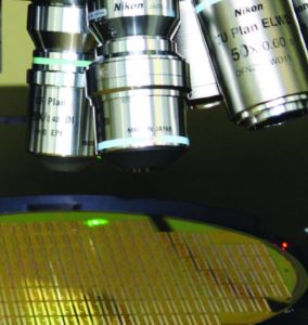
Inside the production



Industries
Processes & technical limits
| Processes | Tolerance | Max. part | Weight | Lot size | Materials |
|---|---|---|---|---|---|
| Macro inspection (BEOL front-end, full-wafer defect inspection)Testing | – | – | – | – | Silicon wafers, Compound semiconductor wafers |
| 2D and 3D inspection and metrology for Advanced PackagingTesting | Sub-micron accuracy (CLIP) | – | – | – | Silicon wafers |
| Post-dicing inspection and metrology (including stealth and plasma dicing processes)Testing | – | – | – | – | Silicon wafers |
| Inspection and metrology for silicon and compound wafers (epitaxial layers, inner cracks,Testing | – | – | – | – | Silicon, Compound semiconductors |
| Panel inspection and metrology for Fan-Out Panel-Level Packaging (FO-PLP)Testing | – | 650 mm × 650 mm | – | – | Panel substrates |
| 3D light interferometry (CLIP) for height/depth measurement of micro bumps, RDLs,Testing | sub-micron (height/depth measurement) | – | – | – | Silicon wafers |
| Layer thickness measurement (sub-micron)Testing | sub-micron | – | – | – | Coated wafers |
| Inner Crack Imaging (detection of inner cracks after dicing)Testing | – | – | – | – | Silicon wafers |
| Backside inspection (wafer backside)Testing | – | – | – | – | Silicon wafers |
| CAD-based inspection (GDSII import for die, reticle, wafer, panel)Testing | – | – | – | – | – |
| Slip line inspection (epitaxial layers)Testing | – | – | – | – | Epitaxial wafers |
5 Anlagen & Maschinen
| Machine | Manufacturer / model | Quantity | Working area | Year built | Site |
|---|---|---|---|---|---|
| Inspection and metrology system (2D/3D, Advanced Packaging) | Camtek Eagleᵀ-AP | – | – | – | – |
| Inspection system | Camtek Eagleᵀ-i | – | – | – | – |
| Inspection system | Camtek Eagleᵀ-i Plus | – | – | – | – |
| Panel inspection and metrology system (up to 650 mm x 650 mm) | Camtek Golden Eagle | – | up to 650 mm x 650 mm | – | – |
| Wafer inspection and metrology platform (Eagle platform) | Camtek Eagle | – | – | – | – |
Additional services
Reference customers
Quality & Certifications
Camtek is certified to ISO 9001 (quality), ISO 14001 (environment) and ISO 45001 (occupational health and safety). The systems inspect and measure wafers with sub-micron accuracy to ensure Known Good Die for defect-free end products.
| Evidence | Migdal Ha'emek |
|---|---|
| ISO 9001 | |
| ISO 14001 | |
| ISO 45001 |
Company History
- 1987–2009
Rafi Amit was CEO and Chairman of the Board; previously President of Priortech since 1981.
- 2011
Moshe Eisenberg joins as Chief Financial Officer.
- 2014
Ramy Langer joins and has been leading the company as COO since November 2017.
- 2017
Orit Geva-Dvash becomes Vice President of Human Resources.
- 2025
Lior Aviram becomes Active Chairman of the Board (since June 1, 2025); Rafi Amit returns as CEO.
- 2026
Acquisition of Visual Layer to deepen Visual AI capabilities in inspection and metrology (April); orders exceeding 105 million US dollars from a Tier-1 OSAT and a leading HBM manufacturer (June); several management appointments in August.