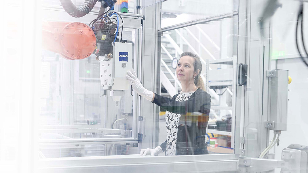
Lithography optics, photomask solutions and wafer metrology for global semiconductor manufacturing.
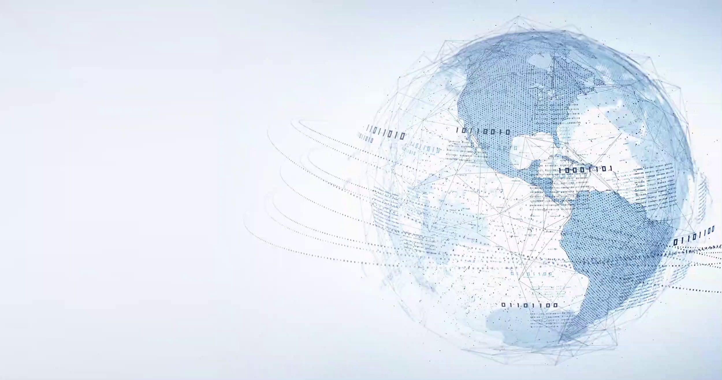
Carl Zeiss SMT GmbH
Oberkochen · Wetzlar · Jena · Rossdorf · Aachen · Coswig · Zürich · Dublin · Bar LevNew on Amplifa
About ZEISS Semiconductor Manufacturing Technology
Carl Zeiss SMT GmbH (Semiconductor Manufacturing Technology) is the semiconductor segment of the ZEISS Group and develops and manufactures precision optics and systems for chip production. The portfolio includes lithography optics for DUV, EUV (13.5 nm) and High-NA-EUV lithography, OEM optic modules for lithography lasers and wafer inspection, photomask solutions (Mask Repair, qualification with AIMS®, metrology with PROVE, Tuning) as well as wafer fab solutions such as 3D X-ray laminography (NLX, 300 mm wafer), wafer shape control (DUNE), multi-beam scanning electron microscopy (MultiSEM) and FIB-SEM 3D metrology with resolutions down to 0.9 nm. Optical components are manufactured and machined from materials including silicon, glass, quartz and calcium fluoride. Around 80 percent of the microchips produced worldwide are made with lithography systems from strategic partner ASML and ZEISS SMT optics. The headquarters is located in Oberkochen (Baden-Württemberg); nine sites in Germany, Switzerland, Ireland and Israel as well as a network of more than 1,200 partners and local service centers in Asia, the USA and Europe complete the company. Customers come from the semiconductor, electronics, automotive and energy industries as well as from research (synchrotron optics).
- Site
- Oberkochen
- Processes
- EUV lithography optics (13.5 nm), DUV lithography optics (365, 248, 193 nm), High-NA-EUV lithography, Synchrotron optics and X-ray gratings, Laser components and modules (calcium fluoride components, metrology modules for excimer lasers), Optics for wafer inspection, Mask repair (repair of hard/soft defects on photomasks, FIB and electron beam methods), Mask qualification (AIMS®)
- Materials
- Silicon (wafer), Glass (photomasks), Quartz (photomasks), Calcium fluoride (optic components), Acetate (frames), Titanium (frames), Silicon (Wafer), Quartz
- Founded
- 1994
- Employees
- 9349
- Industries
- Semiconductor industry, Chip manufacturers, Electronics, Communications, Consumer electronics, Automotive
- 01
Research and Development
- 02
Design and Engineering
- 03
Precision Manufacturing of Optic Components
- 04
System Integration and Assembly
- 05
Metrology and Qualification
- 06
Global Support and Service
Materials and Processes
Silicon (Wafer)
Base material of the wafers onto which nanometer-fine structures are projected.
Quartz
Transparent mask substrate for photomasks.
Glass
Substrate material for photomasks in chip manufacturing.
Calcium Fluoride
Optic components for DUV lithography lasers at 193 and 248 nm.
Sites
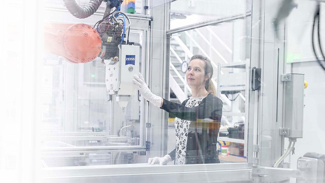
Oberkochen
DEMain site/HQ
- Materials
- Silicon, glass, quartz, calcium fluoride
- EUV/DUV lithography optics manufacturing
- MultiSEM
- 3D Metrology and Inspection Workstation
Wetzlar
DESite
Jena
DESite
Rossdorf
DESite (Mask Solutions, formerly NaWoTec, acquired in 2005)
- Materials
- Glass, quartz
- Mask repair systems
- AIMS® mask qualification system
- PROVE mask metrology system
Aachen
DESite (Philips Engineering Solutions, acquired in 2024)
Coswig
DESite
Zürich
CHSite
Dublin
IESite
Bar Lev
ILSite (Pixer Technology, acquired in 2008)
- Mask tuning systems
Products and Systems
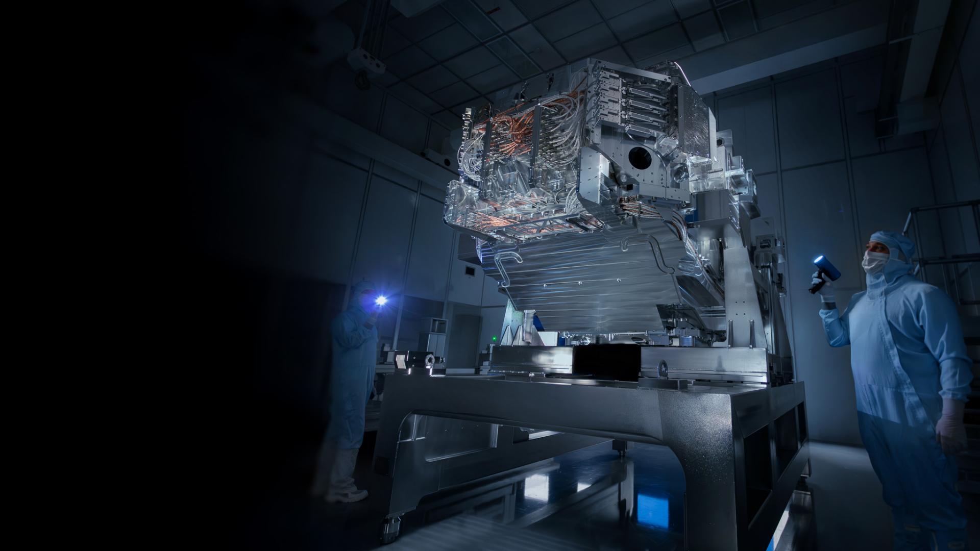
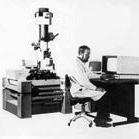
Inside the production
Industries
Processes & technical limits
| Processes | Tolerance | Max. part | Weight | Lot size | Materials |
|---|---|---|---|---|---|
| EUV lithography optics (13.5 nm)Engineering | – | – | – | – | Silicon wafers |
| DUV lithography optics (365, 248, 193 nm)Engineering | – | – | – | – | Silicon wafers |
| High-NA-EUV lithographyEngineering | – | – | – | – | – |
| Synchrotron optics and X-ray gratingsEngineering | – | – | – | – | – |
| Laser components and modules (calcium fluoride components, metrology modules for excimer lasers)Engineering | – | – | – | – | Calcium fluoride |
| Optics for wafer inspectionInspection | – | – | – | – | Silicon |
| Mask repair (repair of hard/soft defects on photomasks, FIB and electron beam methods)Inspection | – | – | – | – | Glass, Quartz |
| Mask qualification (AIMS®)Inspection | – | – | – | – | – |
| Mask metrology (PROVE – positional accuracy of mask structures)Inspection | – | – | – | – | – |
| Mask tuningInspection | – | – | – | – | – |
| Inline 3D X-ray laminography for advanced packaging (300 mm wafer)Inspection | – | – | – | – | Silicon |
| Active wafer shape control (global wafer warpage measurement and correction)Inspection | – | – | – | – | Silicon |
| Multi-beam SEM analysis (2D structure analysis, fault diagnosis, 91 beams)Inspection | – | – | – | – | Silicon |
| FIB tomography (3D volume analysis of microchips, resolution down to 0.9 nm)Inspection | 0.9 nm resolution | – | – | – | Silicon |
7 Anlagen & Maschinen
| Machine | Manufacturer / model | Quantity | Working area | Year built | Site |
|---|---|---|---|---|---|
| 3D X-ray laminography system | ZEISS NLX | – | 300 mm wafer | – | – |
| Wafer shape control system with metrology | ZEISS DUNE 100 | – | – | – | – |
| Multi-beam scanning electron microscope (91 parallel beams, 1.5 TB/h data rate) | ZEISS MultiSEM | – | – | – | – |
| FIB-SEM 3D metrology and inspection workstation (resolution 0.9 nm at 15 keV) | ZEISS 3D Metrology and Inspection Workstation | – | – | – | – |
| Mask qualification system | ZEISS AIMS® | – | – | – | – |
| Mask metrology system | ZEISS PROVE | – | – | – | – |
| Mask repair systems | ZEISS | – | – | – | – |
Additional services
Reference customers
History
- 1846
Founding of ZEISS
- 1968
First ZEISS optics for a circuit plotter (Telefunken) with 15 µm structures
- 1977
World's first wafer stepper with ZEISS optics (S-Planar 10/0.28, David Mann/GCA)
- 1994
Founding of the SMT business segment
- 1997
Strategic partnership with ASML
- 1998
First 193 nm optics
- 2001
Oberkochen site opened
- 2002
ASML and ZEISS SMT become world market leaders
- 2005
NaWoTec GmbH Rossdorf becomes part of ZEISS SMT (Mask Repair)
- 2008
Acquisition of Pixer Technology (Israel)
- 2016
ASML becomes a minority shareholder of ZEISS SMT
- 2017
Founding of ZEISS Process Control Solutions (today Semiconductor Fab Solutions)
- 2018
50 years of ZEISS SMT
- 2019
First chips made with EUV reach the mass market (smartphones)
- 2020
German Future Prize for EUV lithography (ZEISS, TRUMPF, Fraunhofer IOF)
- 2022
20 years of strategic partnership with ASML
- 2023
First High-NA-EUV projection optics and illumination system delivered
- 2024
Acquisition of Philips Engineering Solutions (Aachen) and the lithography division of Beyond Gravity; ASML Supplier Award, KLA Excellence in Technology Award, Werner von Siemens Ring