
Develops systems for the automated integration of nanomaterials such as carbon nanotubes into semiconductor chips at wafer level.

Chiral Nano AG
Dübendorf (Switzerland)New on Amplifa
About Chiral Nano
Chiral Nano AG is a deep-tech company founded in Switzerland in 2023 and a spin-off of ETH Zurich. The company develops semiconductor manufacturing equipment for producing electronic transistors with integrated nanomaterials such as carbon nanotubes (CNTs), TMDs, hBN, graphene and nanowires. The offering includes the Nanodevice Foundry (material growth, material selection, mechanical transfer, device fabrication, as well as electrical and structural characterization), design and process flow support, substrate/wafer fabrication as a service, and the company's own Nanoassembly Equipment for automated CNT integration. Mechanical transfer is performed contamination-free at room temperature and replaces liquid-based deposition methods. The company serves industries such as semiconductor manufacturing, quantum technology, nanoelectronics, photonics and nanofluidics. It is located in Dübendorf near Zurich, with access to a cleanroom at the Binnig and Rohrer Nanotechnology Center (BRNC).
- Site
- Dübendorf
- Processes
- Nanomaterial integration (mechanical transfer of 1D/2D nanomaterials onto wafers), Nanomaterial growth, Nanomaterial characterization, Substrate fabrication (wafer fabrication service), Device design / layout design and process flow, Electrical/structural characterization of devices (e.g. CNT FET room and low temperature, Nanodevice Foundry (material growth, selection, mechanical transfer, device fabrication,, Nanodevice Foundry (material growth, material selection, mechanical transfer, device fabrication)
- Materials
- Carbon nanotubes (CNT), Nanowires, TMDs, hBN, Graphene, Silicon (traditional, comparison basis), 200mm wafers, Carbon Nanotubes
- Founded
- 2023
- Industries
- Semiconductor manufacturing, Quantum technology, Nanoelectronics, Photonics, Nanofluidics
- 01
Device design and process flow
- 02
Substrate/wafer fabrication
- 03
Nanomaterial growth
- 04
Nanomaterial characterization and selection
- 05
Automated mechanical transfer (nanoassembly)
- 06
Electrical/structural characterization
Nanomaterials & Processes
Carbon Nanotubes
1D nanomaterial with high electrical and thermal conductivity for high-performance transistors, interconnects and quantum-dot systems.
Nanowires
Linear 1D structures for transistors, interconnects and nanoscale sensors.
TMDs
Two-dimensional materials with tunable band gaps for ultra-thin transistors and optoelectronics (roadmap).
hBN
Atomically thin 2D dielectric for heterostructures and quantum devices (roadmap).
Graphene
2D nanomaterial for flexible electronics and advanced optoelectronics (roadmap).
200mm Wafers (Silicon)
Substrates as carrier material for wafer-level integration of nanomaterials.
Locations
Dübendorf
CHHeadquarters, office and development; cleanroom access via BRNC
- Part weight / size
- Wafer level (200mm; upgrade path toward 12-inch)
- Lot size
- Prototypes to pilot production
- Materials
- CNTs, nanowires; TMDs, hBN, graphene (roadmap)
- Nanoassembly Equipment (automated CNT transfer, >1,000 assembly motions/h, sub-micron alignment)
Devices & Equipment
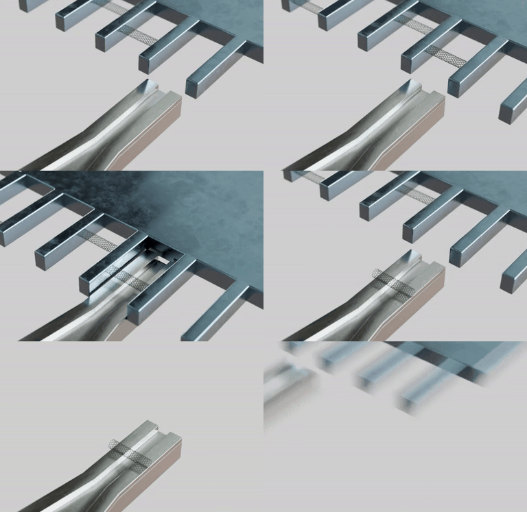
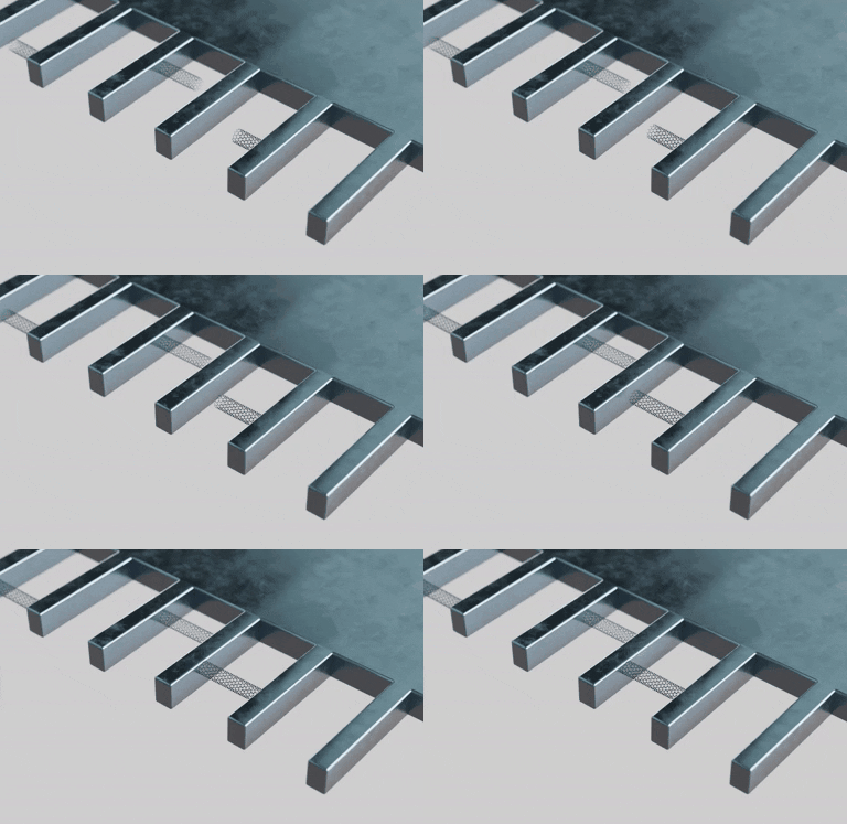
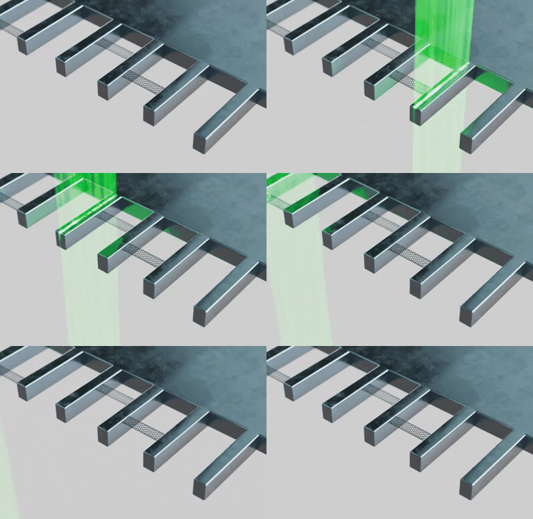
Inside the production






Industries
Processes & technical limits
| Processes | Tolerance | Max. part | Weight | Lot size | Materials |
|---|---|---|---|---|---|
| Nanomaterial integration (mechanical transfer of 1D/2D nanomaterials onto wafers)Assembly | sub-micron alignment accuracy | – | – | – | Carbon Nanotubes, TMDs, hBN, Graphene, Nanowires |
| Nanomaterial growthEngineering | – | – | – | – | Carbon Nanotubes, 2D materials (graphene, hBN, TMDs in roadmap) |
| Nanomaterial characterizationTesting | – | – | – | – | Carbon Nanotubes, nanomaterials |
| Substrate fabrication (wafer fabrication service)Engineering | – | – | – | – | wafers |
| Device design / layout design and process flowEngineering | – | – | – | – | – |
| Electrical/structural characterization of devices (e.g. CNT FET room and low temperatureTesting | – | – | – | – | – |
| Nanodevice Foundry (material growth, selection, mechanical transfer, device fabrication,Assembly | – | – | – | – | Carbon Nanotubes |
2 Anlagen & Maschinen
| Machine | Manufacturer / model | Quantity | Working area | Year built | Site |
|---|---|---|---|---|---|
| Nanoassembly Equipment (automated nanoassembly system for CNT transfer) | Chiral | – | wafer-level (upgrade path toward 12-inch wafer support) | – | Dübendorf, Switzerland |
| Wafer processing machines | – | – | 200mm wafers | – | – |
Additional services
History
- 2023
Founded in Switzerland as a spin-off of ETH Zurich