Ultra-thin, PFAS-free functional polymer coatings via CVD for electronics, sensor technology and medical engineering.

conformally GmbH
Kiel · HeadquartersNew on Amplifa
About conformally
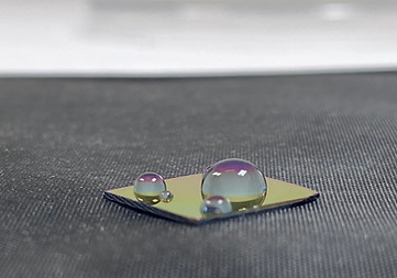
conformally GmbH is a deep-tech company founded in 2025 and a spin-off of the research group of Prof. Franz Faupel at Christian-Albrechts-Universität zu Kiel. The company develops and markets ultra-thin, functional polymer thin films based on its own variants of chemical vapor deposition (CVD), including Initiated CVD (iCVD). These processes enable conformal coating of powders, liquids, solid, highly porous and temperature-sensitive objects while preserving functional groups – unlike conventional processes such as PECVD. The PFAS-free coatings serve as alternatives to fluorinated compounds and are used, among other things, as dielectric layers in microelectronics, as protective and electret layers for sensor components, and as hydrophobic, antiviral or cell-compatible surfaces in medical engineering and biotechnology. In addition to coating development, conformally offers modular CVD reactor systems for integration into production lines as well as process adaptation and optimization. The company is based at the Center for Networked Sensor Systems in Kiel.
- Site
- Kiel
- Processes
- Chemical Vapor Deposition (CVD) – ultra-thin, functional, topographically conformal polymer thin, Initiated Chemical Vapor Deposition (iCVD) – deposition of polymer films with adjustable, Coating development / custom coating solutions, Process adaptation and optimization (scale-up, fine-tuning, integration into existing lines), Dielectric layers for microelectronics (low-k/high-k, flexible electronics, advanced packaging), Protective coating of sensor components (protection against environmental influences, acids,, Electret layer deposition (stable charge storage), Functional surfaces for med-tech/biotechnology (hydrophobization, antiviral properties,
- Materials
- Polymers (organic thin films), PFAS-free coating materials (alternatives to fluorinated compounds), Chemical Vapor Deposition, Initiated Chemical Vapor Deposition, Polymer Thin Films, PFAS-Free Coating Materials
- Certificates
- ISO 9001
- Founded
- 2025
- Industries
- Microelectronics, Semiconductor Technology, Medical Engineering / Med-Tech, Biotechnology, Sensor Technology, Advanced Manufacturing
- 01
Inquiry & Consulting
- 02
Coating Development
- 03
CVD Coating (Prototype/Volume Production)
- 04
Process Optimization & Scale-up
- 05
System Integration / Delivery of Modular CVD Reactors
Materials & Processes
Chemical Vapor Deposition
Vapor-phase deposition of ultra-thin, topographically conformal polymer layers, also on powders, liquids, porous and temperature-sensitive objects.
Initiated Chemical Vapor Deposition
Deposition of polymer films with adjustable polarity and strength of the surface potential, among other things for electret layers.
Polymer Thin Films
Organic functional layers with preserved functional groups for electronics, sensor technology and medical engineering.
PFAS-Free Coating Materials
Alternatives to fluorinated compounds with comparable functionality without regulatory concerns.
Sites
Kiel
DEHeadquarters, development and coating services
- Lot size
- Prototype to volume production
- Materials
- Polymer thin films, PFAS-free coating materials
- Modular CVD coating reactors (standard module reactors for integration into production lines)
Coatings & Applications

Inside the production
Industries
Processes & technical limits
| Processes | Tolerance | Max. part | Weight | Lot size | Materials |
|---|---|---|---|---|---|
| Chemical Vapor Deposition (CVD) – ultra-thin, functional, topographically conformal polymer thinSurface | – | – | – | – | Polymers (organic thin films), temperature-sensitive materials, powders, liquids, solid objects, highly porous objects |
| Initiated Chemical Vapor Deposition (iCVD) – deposition of polymer films with adjustableSurface | – | – | – | – | Polymers |
| Coating development / custom coating solutionsEngineering | – | – | – | – | – |
| Process adaptation and optimization (scale-up, fine-tuning, integration into existing lines)Engineering | – | – | – | – | – |
| Dielectric layers for microelectronics (low-k/high-k, flexible electronics, advanced packaging)Surface | – | – | – | – | Polymers |
| Protective coating of sensor components (protection against environmental influences, acids,Surface | – | – | – | – | Polymers |
| Electret layer deposition (stable charge storage)Surface | – | – | – | – | Polymers |
| Functional surfaces for med-tech/biotechnology (hydrophobization, antiviral properties,Surface | – | – | – | – | Polymers |
1 Anlagen & Maschinen
| Machine | Manufacturer / model | Quantity | Working area | Year built | Site |
|---|---|---|---|---|---|
| Modular CVD coating reactors (standard module reactors for integration into production lines) | conformally | – | – | – | Kiel |
Additional services
Quality
The layers are characterized by high chemical and morphological quality as well as precise surface coverage and are suitable for highly sensitive applications in microelectronics, semiconductor and medical technology.
| Evidence | Kiel |
|---|---|
| ISO 9001 |
History
- 2025
Founded as a deep-tech spin-off of the research group of Prof. Franz Faupel (Kiel University) with support from the EXIST Research Transfer Program; articles of association dated 20.03.2025, entered in the commercial register on 08.05.2025 (HRB 28121 KI).
- 2025
Listed on the Deep Tech Momentum (DTM) Watchlist / DTM100; pitch at Deep Tech Momentum and Shark-Tank session of the International Semiconductor Industry Group.