Electronics manufacturing: prototype assembly, manual placement from 0201 and SMD/THT assembly through to the finished device.

D&S Electronics LTD
Kaufbeuren (P.O. box/administration) · Production facilities Czech RepublicNew on Amplifa
About D&S Electronics
D&S Electronics LTD is a Bavarian electronics service provider (EMS) with its administrative headquarters in Kaufbeuren and production facilities in the Czech Republic. Since 2006 the company has manufactured electronic assemblies: from the circuit diagram through PCB fabrication and material procurement to the populated, tested and ready-to-ship assembly or complete device. The service portfolio covers prototype manufacturing within a few days, manual placement of all package types from 0201 including BGA, QFP and through-hole, automatic SMD placement, THT and mixed assembly for small and volume production, BGA rework with reballing under the microscope using IR technology, as well as reflow soldering, AOI inspection, programming, functional testing and firmware updates. In addition, SMD stencils, PCB repair, device manufacturing, assembly, warehousing and logistics are offered. Customers thus receive a single point of contact for the entire electronics manufacturing process; entrepreneurs in Germany and Europe are supplied.
- Site
- Kaufbeuren
- Processes
- Prototype manufacturing, Manual placement, SMD placement (automatic), THT / through-hole assembly, Mixed assembly (SMD + THT), BGA rework & reballing, BGA/QFN placement, Through-hole construction / free-wired special builds
- Materials
- Printed circuit board / multilayer, Solder paste, SMD/THT components
- Certificates
- AOI inspection, Visual inspection of every solder joint, Functional test & firmware update
- Founded
- 2006-12-11
- Industries
- Electronics/EMS, Development/Prototyping, Small and volume production
- 01
Data intake (circuit diagram, Gerber, BOM)
- 02
Quotation & feasibility check
- 03
Material procurement
- 04
PCB fabrication & SMD stencil manufacturing
- 05
Solder paste printing (stencil)
- 06
SMD/THT/mixed or manual placement
- 07
Reflow soldering
- 08
AOI inspection & visual inspection
- 09
Programming, functional test & firmware update
- 10
Device manufacturing & final assembly
- 11
Warehousing & shipping
Materials & Processes
Printed circuit board / multilayer
Multilayer PCBs form the basis of every populated assembly, built to customer data.
SMD/THT components
Electronically sourced components worldwide from package size 0201 including BGA, QFP and QFN.
Solder paste
Applied reproducibly to the pads via precise SMD stencils and melted in the reflow process.
Locations
Kaufbeuren
DEAdministration & Sales
Czech Republic
CZProduction
- Lot size
- Single piece to series
- Materials
- Printed circuit boards, SMD/THT components
- Automatic SMD placement line (from 0201)
- Reflow ovens
- AOI inspection system
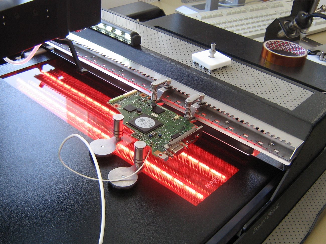
- IR rework station (BGA/reballing)
- Microscope
Components & Assemblies
Inside the production
Industries
Processes & technical limits
| Processes | Tolerance | Max. part | Weight | Lot size | Materials |
|---|---|---|---|---|---|
| Prototype manufacturingAssembly | ±0.03 mm | – | – | Single piece – Small series | – |
| Manual placementAssembly | ±0.03 mm | – | – | Single piece – Small series | – |
| SMD placement (automatic)Assembly | – | – | – | Single piece – Volume production | – |
| THT / through-hole assemblyAssembly | – | – | – | – | – |
| Mixed assembly (SMD + THT)Assembly | – | – | – | – | – |
| BGA rework & reballingAssembly | – | – | – | – | – |
| BGA/QFN placementAssembly | – | – | – | – | – |
| Through-hole construction / free-wired special buildsAssembly | – | – | – | – | – |
| PCB fabrication (board manufacturing)Joining | – | – | – | – | Multilayer PCB |
| SMD stencils (stencil manufacturing)Joining | – | – | – | – | – |
| Reflow solderingJoining | – | – | – | – | – |
| Programming / flashing of components and assembliesTesting | – | – | – | – | – |
| Functional test & firmware updateTesting | – | – | – | – | – |
| AOI inspection / visual inspectionTesting | – | – | – | – | – |
| PCB repair & repair (TFT/plasma monitors, notebooks)Assembly | – | – | – | – | – |
| Device manufacturing & final assembly (cabling, device building)Assembly | – | – | – | – | – |
| Material procurement (BOM)Engineering | – | – | – | – | – |
| Warehousing & logisticsEngineering | – | – | – | – | – |
5 Anlagen & Maschinen
| Machine | Manufacturer / model | Quantity | Working area | Year built | Site |
|---|---|---|---|---|---|
| Automatic placement line (SMD) | – | – | from package size 0201 (metric 0603) | – | Czech Republic (production facilities) |
| Microscope (manual placement/inspection) | – | – | – | – | – |
| IR rework station (BGA replacement/reballing) | – | – | – | – | – |
| AOI inspection system | – | – | – | – | – |
| Reflow ovens | – | – | – | – | – |
Additional services
Quality
Every assembly is tested before it leaves the house: automatic AOI inspection, visual inspection of every solder joint, functional test and firmware update are part of the standard process.
| Evidence | Czech Republic |
|---|---|
| AOI inspection | |
| Visual inspection of every solder joint | |
| Functional test & firmware update |
History
- 2006
Foundation of D&S Electronics LTD on 11.12.2006