Manufacturer of ultra-low-noise pHEMT transistors – from epitaxial design to characterization and device modelling

DIRAMICS AG
Steinhausen, CH · Zurich (founding location)New on Amplifa
About Diramics
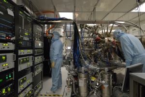
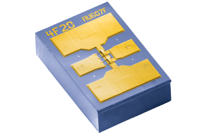
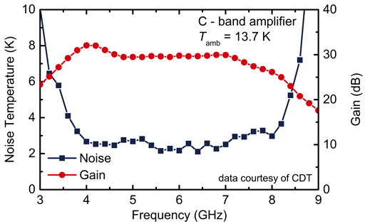
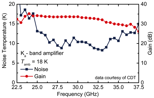
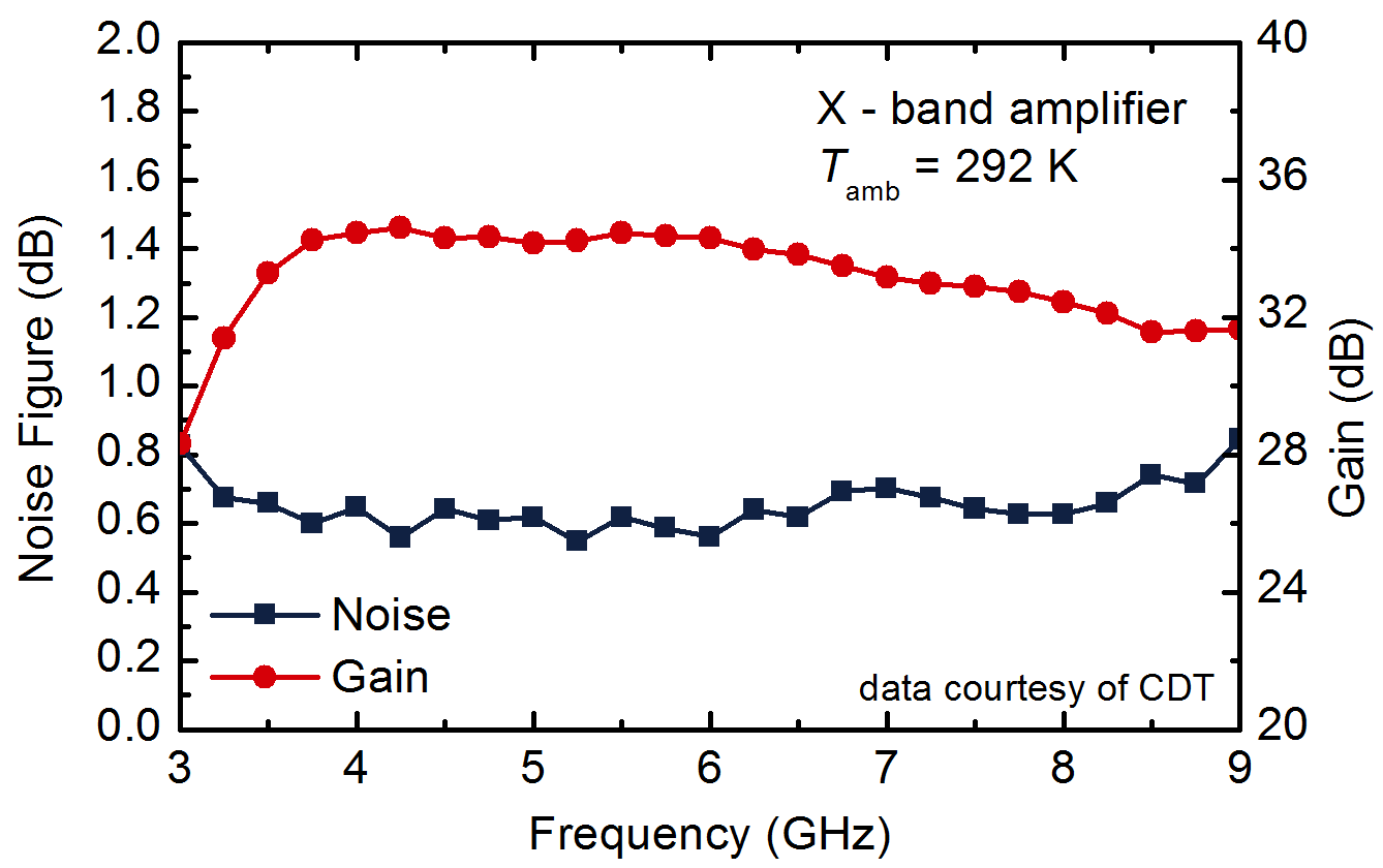
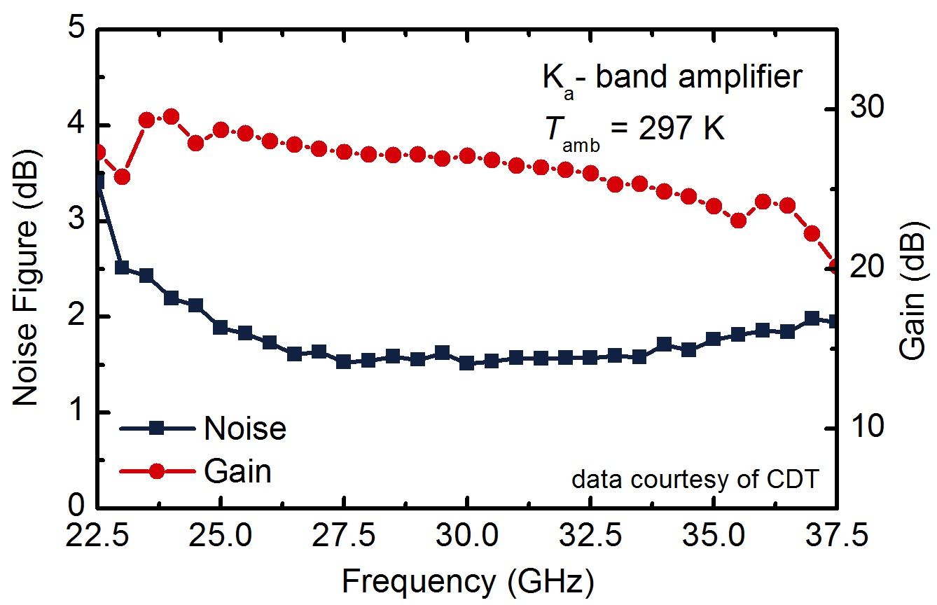
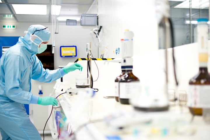
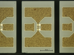
Diramics was founded in 2016 in Zurich as a spin-off of ETH Zurich to bring ultra-low-noise pHEMT technology from research to the market. The company manufactures customizable ultra-low-noise HEMT transistors (pH-100) based on indium phosphide, which have been in field operation at ESA ground stations for more than ten years. The value chain covers all steps: epitaxial layer design (Epi-Design), transistor fabrication in an in-house cleanroom with an MBE system, device characterization and device modelling. The transistors are used in hybrid low-noise amplifiers for radio astronomy and space applications, for example at the Yebes Observatory (IGN/CDT, Spain) and in the Deep Space Network. In 2019, the commercialization of the InP HEMT technology was funded under the EU program Horizon 2020 (Grant Agreement No 855915). The headquarters with production and cleanroom is located in Steinhausen, Switzerland.
- Site
- Steinhausen
- Processes
- Epi-Design (Epitaxial Layer Design), Transistor Fabrication (pHEMT/HEMT Manufacturing), Device Characterization and Modelling, Transistor Fabrication, Device Characterization, Device Modelling, Customizable Ultra-Low-Noise pHEMT Transistors
- Materials
- InP HEMT / pHEMT Technology (Indium Phosphide), Indium Phosphide (InP HEMT / pHEMT), Molecular Beam Epitaxy, Atomic Layer Deposition, Plassys Coating/Etching System
- Certificates
- ISO 9001, Other
- Founded
- 2016
- Industries
- Semiconductors, Space/Ground Stations (ESA), Radio Astronomy, Microwave Technology, Cryogenic Receivers
- 01
Epi-Design (Epitaxial Layer Design)
- 02
MBE Epitaxy
- 03
Transistor Fabrication (Cleanroom)
- 04
Device Characterization
- 05
Device Modelling
Technology & Processes
Indium Phosphide (InP HEMT / pHEMT)
Substrate and semiconductor technology for ultra-low-noise HEMT transistors in microwave and cryogenic applications.
Molecular Beam Epitaxy
Epitaxial process for growing the crystal layers according to the in-house Epi-Design.
Atomic Layer Deposition
Thin-film deposition in the cleanroom for transistor fabrication.
Plassys Coating/Etching System
Vacuum coating and etching of process-critical layers.
Locations
Steinhausen
CHHeadquarters, Production, Cleanroom, Characterization
- Lot size
- Prototype, small series
- Materials
- InP
- MBE System (Molecular Beam Epitaxy)
- Plassys Coating/Etching System
- ALD System (Atomic Layer Deposition)
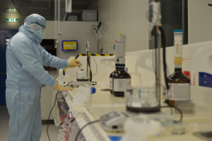
- Wet Bench (Wet Chemistry)
- Wet Chemistry Cleanroom Area
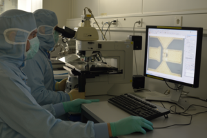
- Microscope
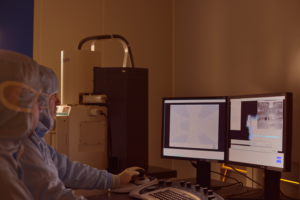
- Scanning Electron Microscope (SEM)
Components & Products
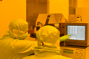
Inside the production

Industries
Processes & technical limits
| Processes | Tolerance | Max. part | Weight | Lot size | Materials |
|---|---|---|---|---|---|
| Epi-Design (Epitaxial Layer Design)Engineering | – | – | – | – | InP |
| Transistor Fabrication (pHEMT/HEMT Manufacturing)Additive | – | – | – | – | InP |
| Device Characterization and ModellingTesting | – | – | – | – | InP |
7 Anlagen & Maschinen
| Machine | Manufacturer / model | Quantity | Working area | Year built | Site |
|---|---|---|---|---|---|
| MBE System (Molecular Beam Epitaxy) | – | – | – | – | Steinhausen, Switzerland |
| Plassys Coating/Etching System | Plassys | – | – | – | Steinhausen, Switzerland |
| Microscope | – | – | – | – | Steinhausen, Switzerland |
| Wet Bench (Wet Chemistry) | – | – | – | – | Steinhausen, Switzerland |
| ALD System (Atomic Layer Deposition, Cleanroom) | – | – | – | – | Steinhausen, Switzerland |
| Wet Chemistry Cleanroom Area | – | – | – | – | Steinhausen, Switzerland |
| Scanning Electron Microscope (SEM) | – | – | – | – | Steinhausen, Switzerland |
Additional services
Reference customers
Quality
Characterization and device modelling are part of the integrated value chain; measurement data of the devices and amplifier modules are published.
| Evidence | Steinhausen |
|---|---|
| ISO 9001 | |
| Other |
History
- 2016
Founded in Zurich as a spin-off of ETH Zurich to commercialize the ultra-low-noise pHEMT technology
- 2019
EU funding under Horizon 2020 (Grant Agreement No 855915) for the commercialization of the InP HEMT technology
- 2025
Website update; pH-100 transistors >10 years in field operation at ESA ground stations