Dicing-Grinding Service for wafers: Ultra-precise dicing, grinding, polishing, laser processes and metrology for semiconductors, MEMS and LEDs.

DISCO HI-TEC EUROPE GmbH
Kirchheim near MunichNew on Amplifa
Wafer processing as a supply chain partner
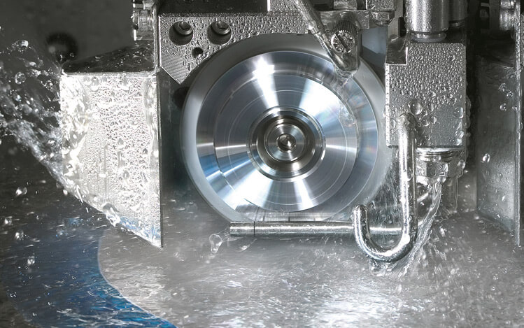
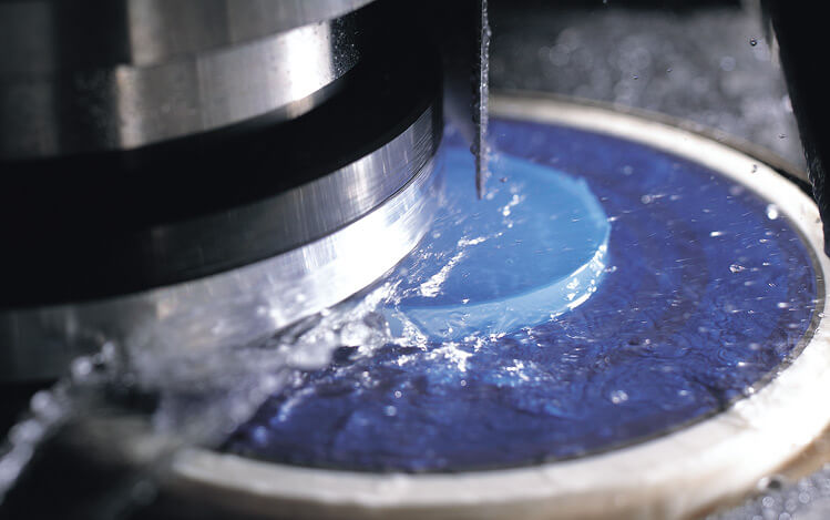
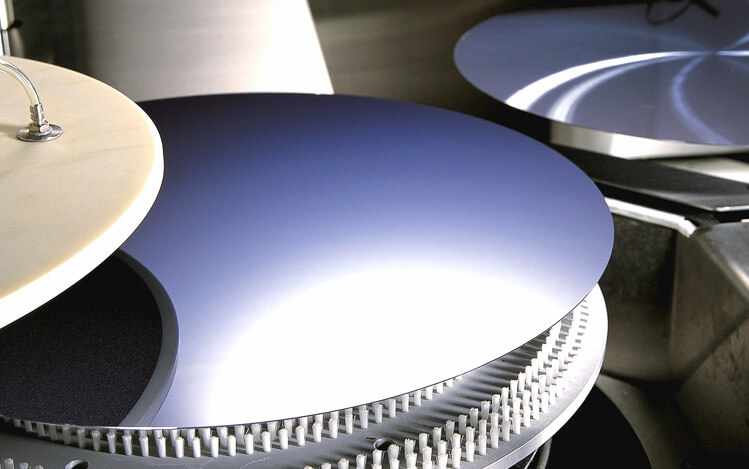
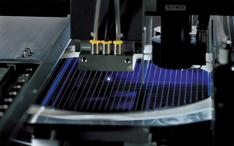
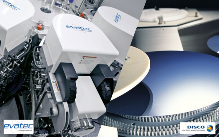
DGS – Dicing-Grinding Service of DISCO HI-TEC EUROPE GmbH performs precision machining tasks in semiconductor production as a supply chain partner: dicing (Kiru), grinding (Kezuru), polishing (Migaku), laser processes, advanced processes as well as metrology and inspection. The range of services spans application support, improvement of existing processes and prototype development through to mass production – with more than 12,000 wafers processed per month (since 2016). Materials processed include silicon and other semiconductors, sapphire, quartz, glass, compound and bonded materials, GaAs, SiC, ceramics, QFN/leadframe, FR4 and further materials on request. Processes include, among others, single/step/bevel cut, pattern grooving, ultrasonic dicing, stealth dicing (also for SiC), DBG/SDBG, TAIKO, Poligrind, dry polishing, plasma etching and stress-relief processes. Production takes place in the cleanroom in Kirchheim near Munich in a 2-shift operation, 7 days per week; since 2019 there has been a partnership with Evatec AG for the sputtering post-process.
- Site
- Kirchheim b. München
- Processes
- Dicing, Grinding, Polishing, Laser, Advanced Processes, Metrology, Single wafer grinding, Partial wafer grinding
- Materials
- Silicon, Sapphire, Quartz, Glass, Bonded Materials, GaAs, SiC, Ceramics
- Certificates
- DIN EN ISO 9001, DIN EN ISO 14001
- Founded
- 2006 (star
- Industries
- Semiconductors, Microsystems technology (MEMS), LED
- 01
Inquiries/Application Support
- 02
Prototype development
- 03
Dicing
- 04
Grinding
- 05
Polishing
- 06
Laser processes
- 07
Advanced Processes
- 08
Metrology & Inspection
- 09
Mass production
Materials and processes
Silicon and other semiconductors
Main material for dicing, grinding, polishing and laser processes.
SiC
Processable, among others, with stealth dicing.
GaAs
Semiconductor material for dicing applications.
Sapphire
Hard substrate material, among others in the LED sector.
Quartz
Substrate material for dicing and grinding.
Glass
For dicing, grinding and polishing.
Ceramics
Brittle material for precision machining.
Bonded Materials
Composite substrates for multilayer processes.
QFN / Lead frame
Package and leadframe materials for singulation.
FR4
Printed circuit board material for dicing and step cut.
Compound materials
Multilayer composite materials, among others for step cut and ultrasonic dicing.
Site
Kirchheim near Munich
DEDicing-Grinding Service with cleanroom production, application support and prototype development
- Lot size
- Prototypes to mass production
- Materials
- Silicon, sapphire, quartz, glass, GaAs, SiC, ceramics, composite materials, FR4, QFN/leadframe
- Cleanroom (1,330 m² including 800 m² extension)
- DISCO precision machines for dicing and grinding
- 3D surface metrology
- Atomic Force Microscope (AFM)
- Automated Optical Inspection (AOI)
Components
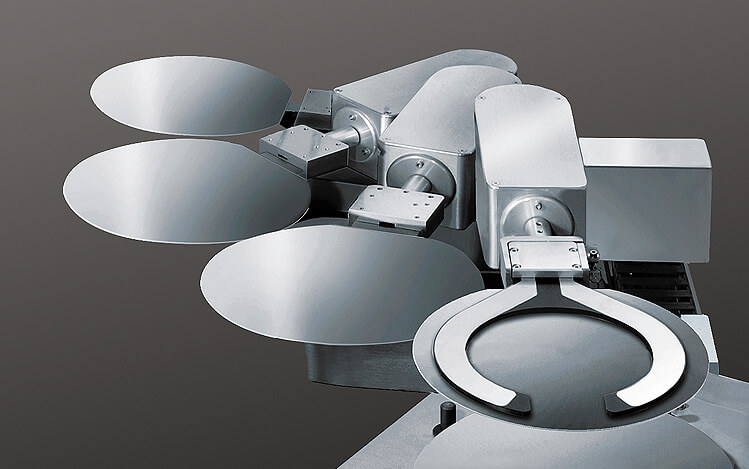
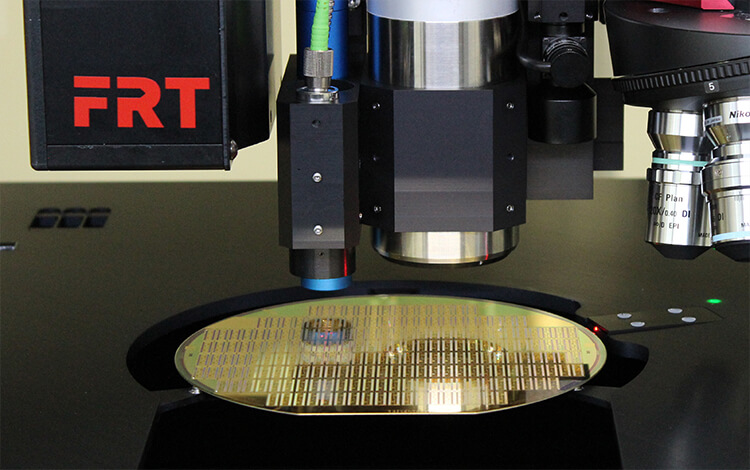
Inside the production
Industries
Processes & technical limits
| Processes | Tolerance | Max. part | Weight | Lot size | Materials |
|---|---|---|---|---|---|
| DicingMachining | – | – | – | – | Silicon, Sapphire, Quartz, Glass, GaAs, SiC, Ceramics, Composite materials |
| GrindingMachining | – | – | – | – | Silicon, SiC, Glass, Ceramics |
| PolishingSurface | – | – | – | – | Silicon, Glass, Sapphire |
| LaserMachining | – | – | – | – | Silicon, SiC |
| Advanced ProcessesOther | – | – | – | – | – |
| MetrologyTesting | – | – | – | – | – |
| Single wafer grindingMachining | – | – | – | – | Silicon |
| Partial wafer grindingMachining | – | – | – | – | Silicon |
| Individual (die) chip grindingMachining | – | – | – | – | Silicon |
| Edge trimming (by grinding)Machining | – | – | – | – | Silicon |
| Poligrind/UltrapoligrindMachining | – | – | – | – | Silicon |
| TAIKOMachining | – | – | – | – | Silicon |
| Single Cut (Dicing)Machining | – | – | – | – | Silicon, SiC, GaAs, Glass |
| Step CutMachining | – | – | – | – | Composite materials |
| Bevel CutMachining | – | – | – | – | Silicon |
| Pattern GroovingMachining | – | – | – | – | Silicon |
| Chopper CutMachining | – | – | – | – | Silicon |
| Circle CutMachining | – | – | – | – | Silicon |
| Ultrasonic DicingMachining | – | – | – | – | Composite materials |
| Stealth dicing (SD)Machining | – | – | – | – | Silicon |
| Stealth dicing of SiCMachining | – | – | – | – | SiC |
| Laser ablationMachining | – | – | – | – | Silicon |
| Laser groovingMachining | – | – | – | – | Silicon |
| Die attach film (DAF) cutMachining | – | – | – | – | Composite materials |
| Dicing before grinding (DBG)Machining | – | – | – | – | Silicon |
| Stealth dicing before grinding (SDBG)Machining | – | – | – | – | Silicon |
| Plasma etchingSurface | – | – | – | – | Silicon |
| Dry polishingSurface | – | – | – | – | Silicon |
| Chemical-mechanical polishingSurface | – | – | – | – | Silicon |
| Stress relief process (higher die strength, warpage reduction)Surface | – | – | – | – | Silicon |
| Surface planarizationSurface | – | – | – | – | Silicon |
| 3D surface metrology systemTesting | – | – | – | – | – |
| Atomic Force Microscopy (AFM)Testing | – | – | – | – | – |
| Automated Optical Inspection (AOI)Testing | – | – | – | – | – |
| Sputtering post process (partnership Evatec AG)Surface | – | – | – | – | – |
3 Anlagen & Maschinen
| Machine | Manufacturer / model | Quantity | Working area | Year built | Site |
|---|---|---|---|---|---|
| 3D surface metrology system | – | – | – | – | Kirchheim near Munich |
| Atomic Force Microscope (AFM) | – | – | – | – | Kirchheim near Munich |
| Automated Optical Inspection (AOI) | – | – | – | – | Kirchheim near Munich |
Additional services
Reference customers
Quality
The quality management system is certified to DIN EN ISO 9001 and DIN EN ISO 14001; all processes are subject to strict controls. For testing, 3D surface metrology, AFM and AOI are available.
| Evidence | Kirchheim near Munich |
|---|---|
| DIN EN ISO 9001 | |
| DIN EN ISO 14001 |
History
- 2006
Start of the Dicing-Grinding Service (DGS) at DISCO HI-TEC EUROPE in Munich
- 2009
Cleanroom extension due to increasing requirements and capacity limits
- 2013
Further cleanroom extension
- 2016
More than 12,000 wafers processed per month
- 2018
Cleanroom extension by 800 m², total processing area 1,330 m²; 2-shift operation 7 days per week
- 2019
Partnership with Evatec AG for the sputtering post-process