Turn-key development and design of ASICs, SoCs, FPGAs, image processing and embedded products.
Dream Chip Technologies GmbH
Garbsen (Hanover) · Hamburg · Lehre-Wendhausen (Braunschweig) · Duisburg · Waalre (Eindhoven, NL)New on Amplifa
About Dream Chip Technologies
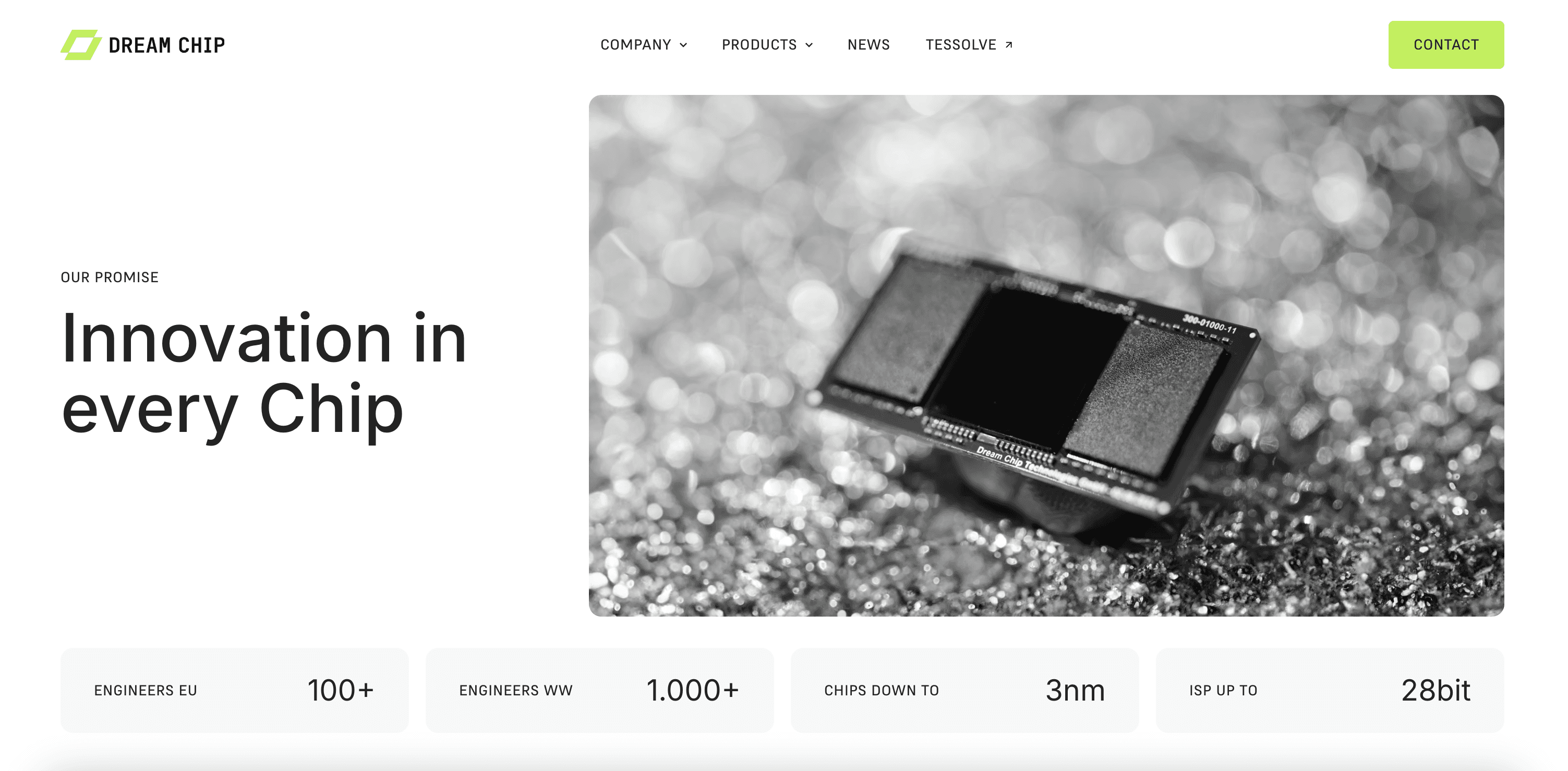
Dream Chip Technologies is an independent engineering turn-key service provider based in Garbsen near Hanover, specializing in the development and design of ASICs, SoCs, FPGAs, embedded software and complex systems. The company covers the entire custom SoC design process – from the idea through the architecture phase to tape-out and post-silicon bring-up – working with chip geometries down to 3 nm. A key focus is image processing: the company develops FuSa-certified ISP solutions with up to 28 bit dynamic range, miniature HDR-capable camera products (Atom Camera) and custom Vision SoCs. Its customers come from the automotive industry, the HPC/data center environment, broadcast, consumer, industrial and medical technology. As part of the Tessolve Group with a total of 1,100 engineers worldwide, Dream Chip offers end-to-end semiconductor solutions from architecture to mass production.
- Site
- Garbsen
- Processes
- ASIC design (development and design), SoC design (turnkey from specification to tape-out and post-silicon testing), FPGA development, Embedded software development, Image processing / ISP development (up to 28 bit dynamic range, FuSa-certified ASIL B/ASIL D), Development of miniature HDR camera products (Atom Camera), Chip design down to 3nm, Development of complex systems / end-to-end semiconductor solutions from architecture to mass
- Materials
- Silicon (chips down to 3nm), Silicon (chips down to 3 nm)
- Certificates
- ISO 9001, TISAX, ISO 26262 (ISP certified ASIL B random faults / ASIL D systematic, TISAX (ENX), ISO 26262 (TÜV Süd, ASIL B/D)
- Employees
- 155+ (EU engineers)
- Industries
- Automotive, HPC/Data Center, Broadcast, Consumer, Industrial, Medical
- 01
Specification
- 02
Architecture
- 03
Chip/SoC design
- 04
Tape-out
- 05
Post-silicon testing
- 06
Embedded software & system development
Technologies & Processes
Silicon (chips down to 3 nm)
Design of ASICs and SoCs in state-of-the-art silicon technologies down to 3 nm structure width.
Locations
Garbsen (Hanover)
DEHeadquarters
Hamburg
DEOffice
Lehre-Wendhausen (Braunschweig)
DEOffice
Duisburg
DEOffice
Waalre (Eindhoven)
NLOffice
Products & Services
Inside the production
Industries
Processes & technical limits
| Processes | Tolerance | Max. part | Weight | Lot size | Materials |
|---|---|---|---|---|---|
| ASIC design (development and design)Engineering | – | – | – | – | Silicon |
| SoC design (turnkey from specification to tape-out and post-silicon testing)Engineering | – | – | – | – | Silicon |
| FPGA developmentEngineering | – | – | – | – | – |
| Embedded software developmentEngineering | – | – | – | – | – |
| Image processing / ISP development (up to 28 bit dynamic range, FuSa-certified ASIL B/ASIL D)Engineering | – | – | – | – | – |
| Development of miniature HDR camera products (Atom Camera)Engineering | – | – | – | – | – |
| Chip design down to 3nmEngineering | – | – | – | – | Silicon |
| Development of complex systems / end-to-end semiconductor solutions from architecture to massEngineering | – | – | – | – | – |
Additional services
Quality & Certifications
The processes are certified to ISO 9001; in addition, there is a TISAX certification (ENX) for data security. ISP development is certified by TÜV Süd to ISO 26262 (ASIL B for Random Faults, ASIL D for Systematic Capabilities).
| Evidence | Garbsen (Hanover) |
|---|---|
| ISO 9001 | |
| TISAX (ENX) | |
| ISO 26262 (TÜV Süd, ASIL B/D) |
History
Dream Chip Technologies is officially part of the Tessolve Group.