
Develops and manufactures custom measurement systems and software for semiconductors, microelectronics and materials testing down to the subnanometer range.

E+H Metrology GmbH
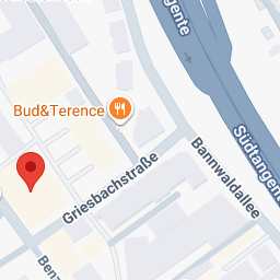
76185 Karlsruhe · Griesbachstraße 12 · Benzstraße 5-9New on Amplifa
About E+H Metrology
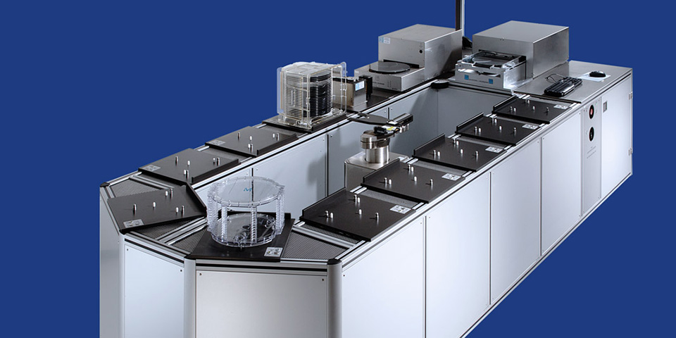
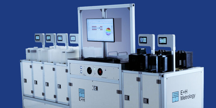
E+H Metrology GmbH is an independent, medium-sized company based in Karlsruhe that has been developing custom measurement systems and software for the limits of measurability since 1968. The portfolio includes capacitive distance sensors, geometry measurement heads, manual measuring devices (Manual Tools), OEM-integrated tools as well as automated measurement systems and wafer sorters (Robot Sorter, Belt Sorter MX 202 WaferStream) for thickness, flatness and surface measurement. Measured materials include silicon wafers, conductive substrates, photovoltaic products, technical ceramics and other materials down to the subnano range, including electrical properties, material properties and cryogenic measurements below approximately -150 °C. Electronics, mechanics, design and software development are carried out entirely in-house; manufacturing takes place at the Karlsruhe site. Customers come from the semiconductor and MEMS industries, microelectronics, research and development, wafer reclaim, technical ceramics, mechanical engineering, sensor technology, as well as photovoltaics and solar. A worldwide network of distributors and partners supports customers locally.
- Site
- Karlsruhe
- Processes
- Contract Measurements, Surface measurement: waviness, saw marks, roughness, nanotopography, Geometry measurement: thickness, TTV (total thickness variation), warp and bow, film stress, Measurement of electrical properties: resistivity, sheet resistance, P/N doping, Measurement of axles, shafts and bearings: shaft displacement in plain bearings, axle concentricity, Turbine and motor measurement, Measurement of material properties: elastic modulus (Young's modulus), thermal expansion coefficient, Low-temperature / cryogenic measurements (below approx. -150 °C) with capacitive sensors
- Materials
- Silicon (wafers), technical ceramics, Photovoltaic products, conductive substrates, Cryogenic materials
- Certificates
- Reproducible measurement according to international calibration standards, Factory calibration / reference wafers (thickness, specific resistivity), ISO 9001 (certified)
- Founded
- 1968
- Industries
- Semiconductors & MEMS, Microelectronics, Research & Development, Wafer Reclaim, Technical Ceramics, Mechanical Engineering
- 01
Consulting and requirements analysis
- 02
Design and electronics/mechanics development (in-house)
- 03
Software development (in-house)
- 04
Manufacturing at the Karlsruhe site
- 05
Calibration to international standards
- 06
Technical support and service
Measurement Methods and Materials
Silicon (wafers)
Thickness, flatness and surface measurement of silicon wafers for semiconductors and photovoltaics.
conductive substrates
Geometry measurement heads measure the thickness and properties of conductive substrates.
technical ceramics
Measurement systems for components and materials of the ceramics industry.
Photovoltaic products
Measurement solutions for wafers and products of the photovoltaic and solar industry.
Cryogenic materials
Capacitive sensors with nanometer resolution for measurements below approx. -150 °C.
Locations
Karlsruhe
DEHeadquarters: development, production, metrology, electronics, mechanics, design, sales, administration
- Materials
- Silicon, conductive substrates, technical ceramics
- Robot Sorter MX2012 (wafer robot sorter)
- Belt Sorter MX 202 WaferStream
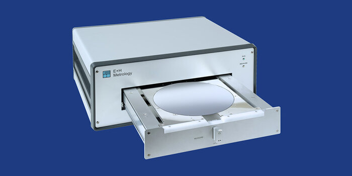
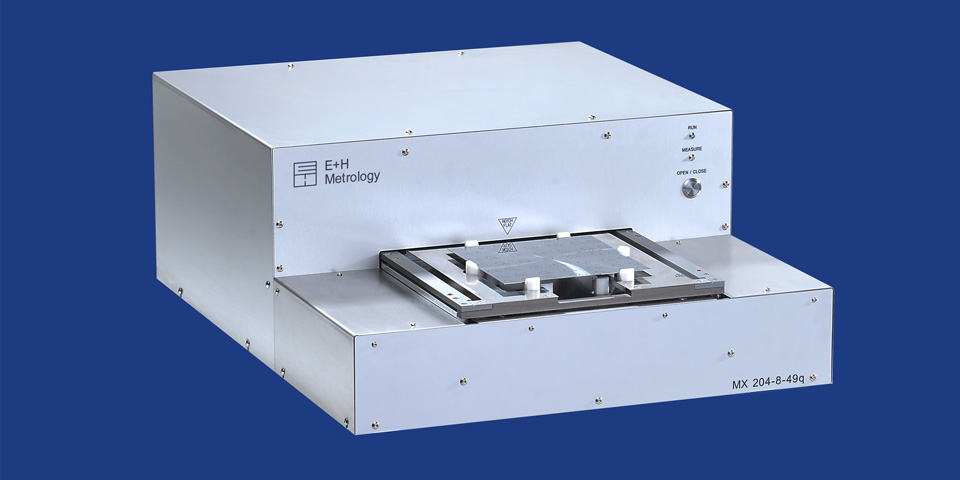
- Manual Tools (MX203, MX204)
- OEM Integrated Tools (MX152)
- Automated Tools (MX204, MX608)
- Sensor Systems (Standard Sensors, Distance Meters)
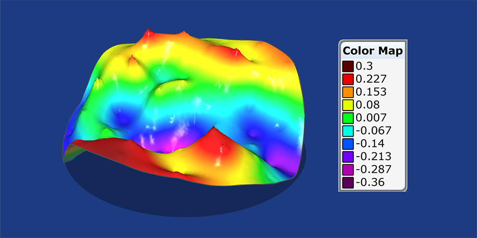
- GNS Global Nanoscope (Makyoh technology)
Products and Systems
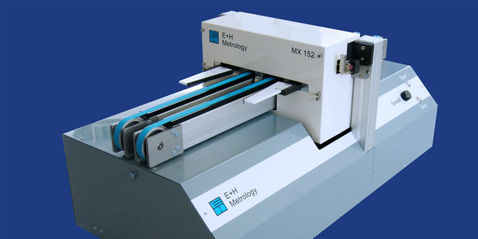
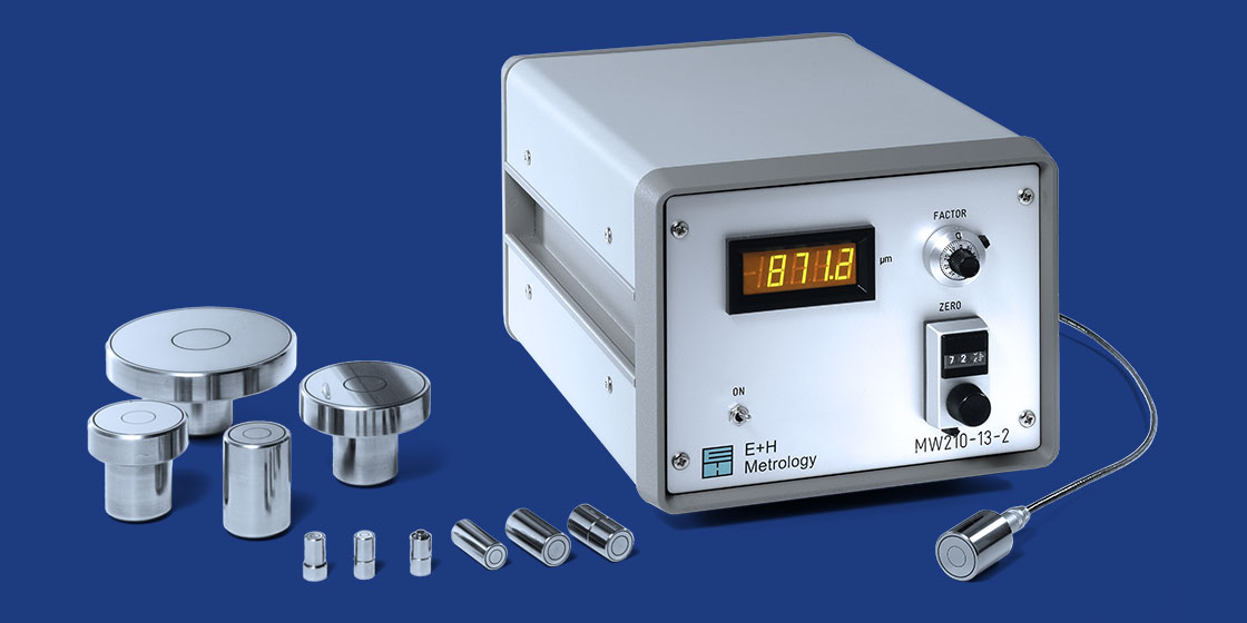
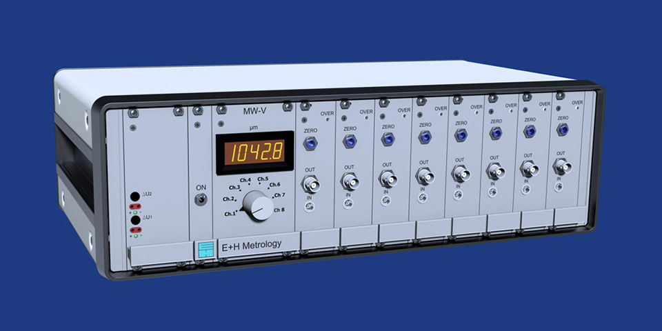
Inside the production
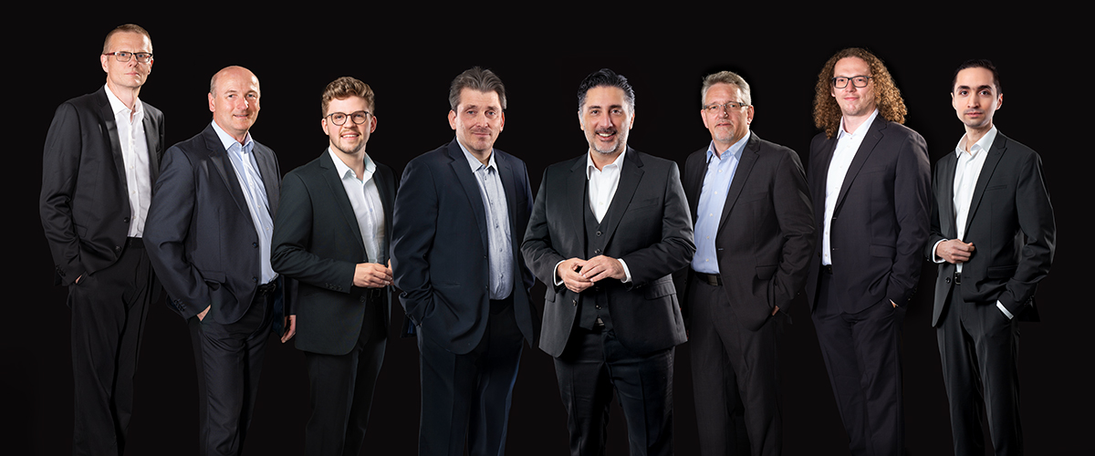
Industries
Processes & technical limits
| Processes | Tolerance | Max. part | Weight | Lot size | Materials |
|---|---|---|---|---|---|
| Contract MeasurementsTesting | – | – | – | – | Wafers, Silicon, technical ceramics, Materials in the subnano range |
| Surface measurement: waviness, saw marks, roughness, nanotopographyTesting | Roughness | – | – | – | Wafers |
| Geometry measurement: thickness, TTV (total thickness variation), warp and bow, film stressTesting | – | – | – | – | Wafers |
| Measurement of electrical properties: resistivity, sheet resistance, P/N dopingTesting | – | – | – | – | Wafers (semiconductors) |
| Measurement of axles, shafts and bearings: shaft displacement in plain bearings, axle concentricityTesting | – | – | – | – | Metal (axles, shafts) |
| Turbine and motor measurementTesting | – | – | – | – | – |
| Measurement of material properties: elastic modulus (Young's modulus), thermal expansion coefficientTesting | Deformations in the nanometer range | – | – | – | Dynamic materials, A wide variety of materials |
| Low-temperature / cryogenic measurements (below approx. -150 °C) with capacitive sensorsTesting | Nanometer resolution | – | – | – | Cryogenic materials, Materials for aerospace, medicine, research |
| Wafer calibration: reference wafers for thickness or specific resistivity, periodic (re)calibrationTesting | – | – | – | – | Silicon wafers, Reference material |
| Thickness measurement of silicon wafers or conductive substrates (Geometry Head)Testing | – | – | – | – | Silicon, conductive substrates |
| Manufacture of custom measurement systems (electronics, mechanics, design, software)Engineering | – | – | – | – | – |
11 Anlagen & Maschinen
| Machine | Manufacturer / model | Quantity | Working area | Year built | Site |
|---|---|---|---|---|---|
| Robot Sorter (wafer robot sorter) | E+H Metrology | – | – | – | Karlsruhe |
| Belt Sorter (modular belt sorter) | E+H Metrology MX 202 WaferStream | – | – | – | Karlsruhe |
| Thickness and flatness gauge 300 mm | E+H Metrology | – | – | 1996 | – |
| 450 mm Tool | E+H Metrology | – | – | 2008 | – |
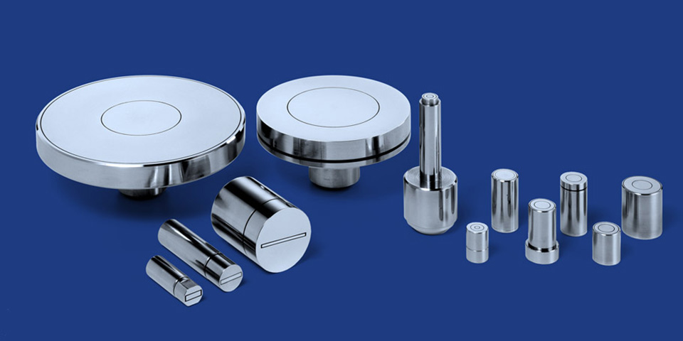
| Capacitive distance sensor / capacitive displacement transducer | E+H Metrology | – | – | – | Karlsruhe |
| Deflectometric measurement technology (AMA Innovation Award) | E+H Metrology | – | – | 2015 | – |
| Makyoh technology (GNS Global Nanoscope) | E+H Metrology GNS Global Nanoscope | – | – | 2021 | – |
| Manual Tools (manual measuring devices) | E+H Metrology | – | – | – | – |
| OEM Integrated Tools | E+H Metrology | – | – | – | – |
| Automated Tools (automated measurement systems) | E+H Metrology MX204, MX608 | – | – | – | – |
| Sensor systems / Distance Meters (Standard Sensors) | E+H Metrology | – | – | – | – |
Additional services
Quality and Calibration
The products deliver reproducible results according to international calibration standards. In-house factory calibration services provide reference wafers for thickness and resistivity, periodic recalibrations and calibration of customer-owned materials.
| Evidence | Karlsruhe |
|---|---|
| Reproducible measurement according to international calibration standards | |
| Factory calibration / reference wafers (thickness, specific resistivity) | |
| ISO 9001 (certified) |
Company History
- 1968
Founding of E+H by Wilfried Eichhorn and Taddaeus Hausmann: linear capacitive distance sensor with cable capacitance elimination.
- 1978
First geometry measurement head for one of the first semiconductor applications: thickness measurement of silicon wafers
- 1992
E+H at the forefront of technological development for the photovoltaic industry
- 1996
First 300-mm thickness and flatness measurement devices presented at SEMICON Europa
- 2001
After 33 years, Wilfried Eichhorn hands over the management of the company to Daniel Raseghi
- 2008
First company with a 450-mm tool at SEMICON 2008
- 2015
AMA Innovation Award for pioneering deflectometric measurement technology
- 2021
Move to new, larger premises at the Karlsruhe site (development, production, testing technology, support)
- 2021
GNS Global Nanoscope: Makyoh technology reimagined
- 2022
E+H Metrology relaunch (website)