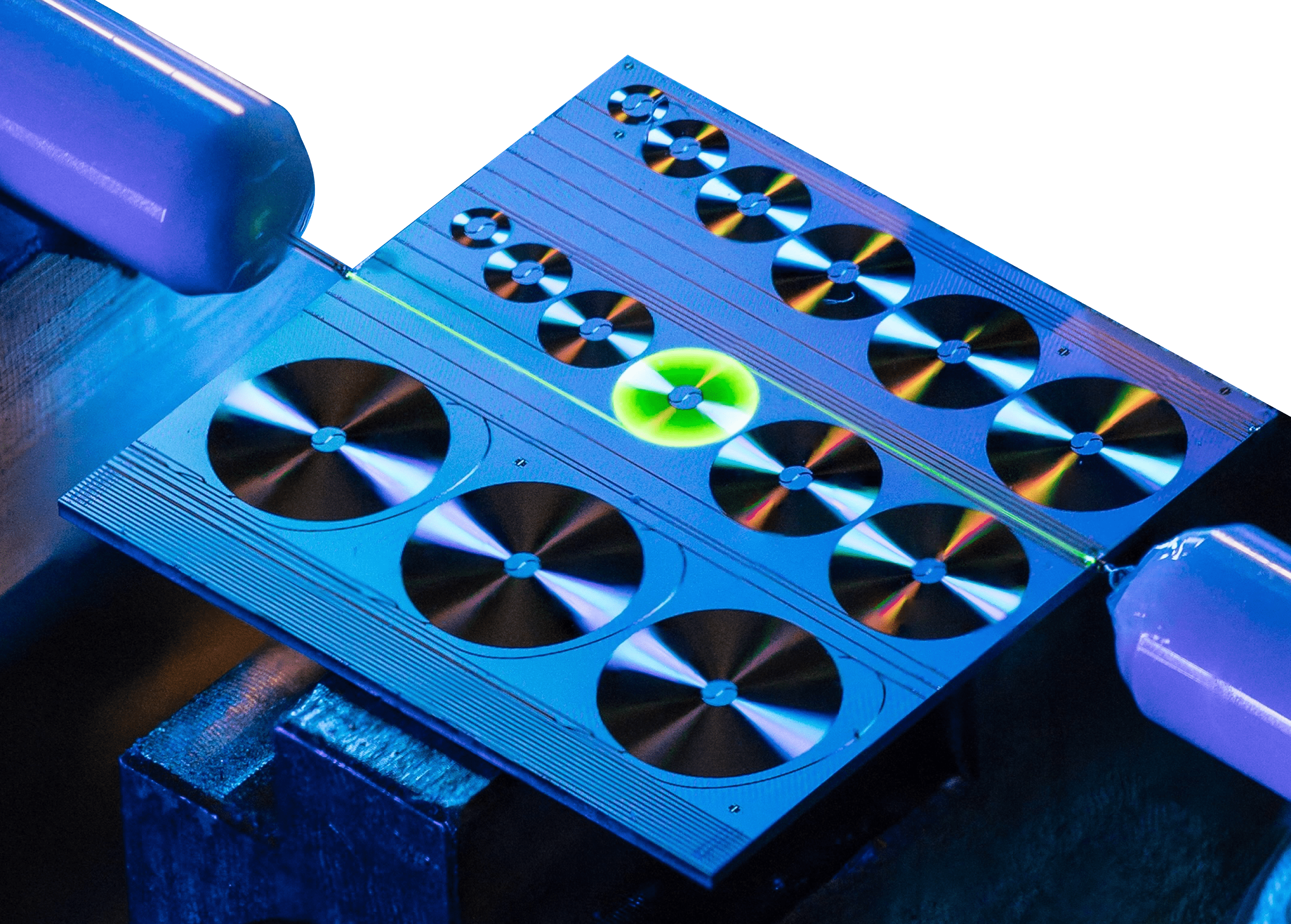
Swiss manufacturer of erbium-doped photonic integrated circuits (EDWA/EDWL) for chip-level optical amplification and lasers.

EDWATEC SA
Lausanne (EPFL Innovation Park)New on Amplifa
About EDWATEC
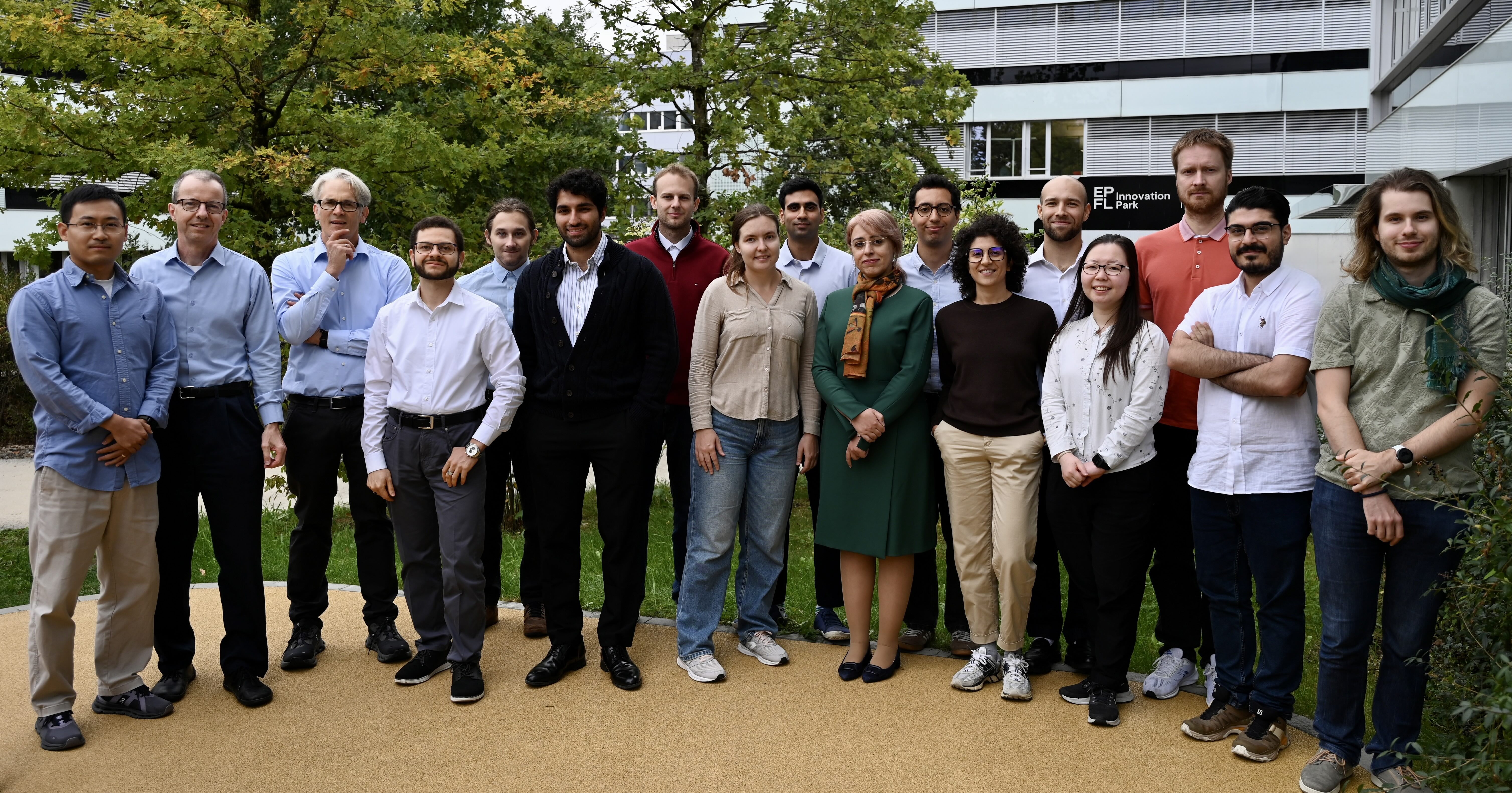
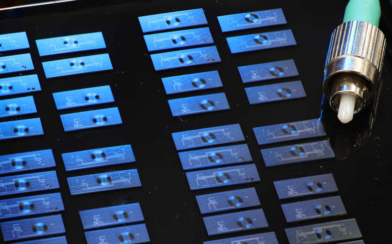
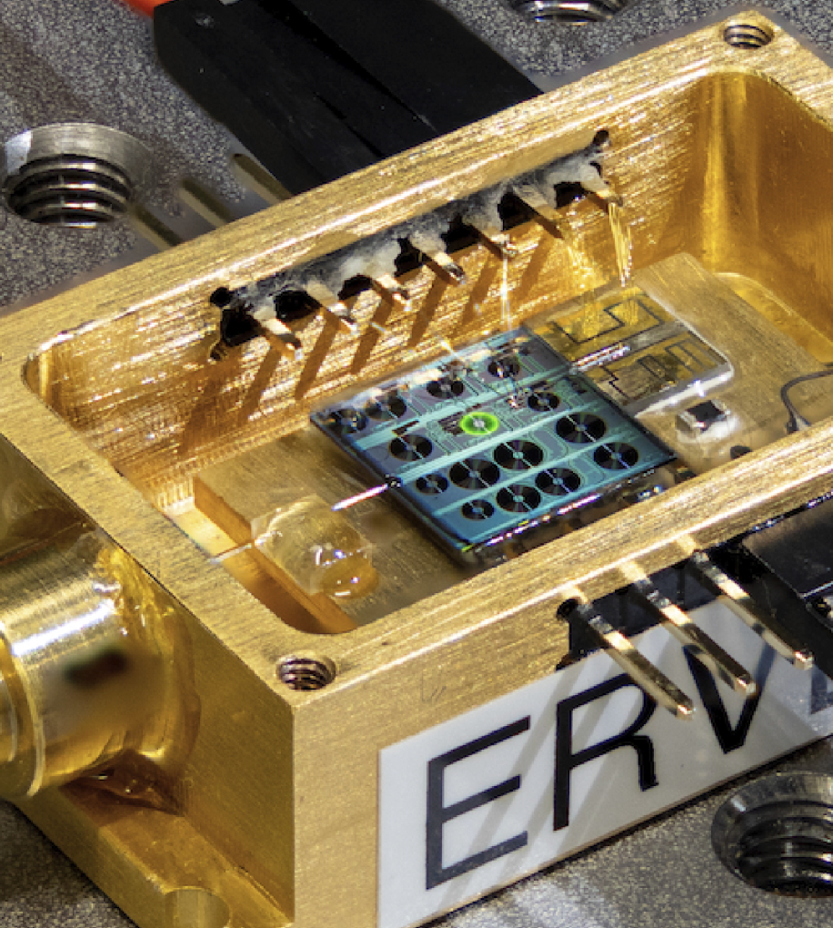
EDWATEC SA is a Swiss high-tech startup that manufactures rare-earth-doped photonic integrated circuits (PICs). Its core products are erbium-doped waveguide amplifiers (EDWA) with 30 dB on-chip gain, 300 mW output power and a noise figure below 5 dB, as well as erbium-doped waveguide lasers (EDWL) with linewidths below 50 Hz, tunable across the C+L bands. The technology is based on low-loss silicon nitride waveguides doped with erbium via controlled ion implantation; production is carried out at wafer level and is compatible with silicon photonics foundry processes for monolithic and hybrid integration. EDWATEC sees itself as an Integrated Device Manufacturer (IDM) and covers the entire R&D cycle – design, nanofabrication and characterization – in-house, with direct access to the nanofabrication facilities of the EPFL Center of MicroNanoTechnology (CMi). Customer industries include optical transceivers, data centers and telecommunications, fiber sensing, satellite communications, and spectroscopy. The company was founded in 2023 as a spin-off of the Laboratory of Photonics and Quantum Measurements (LPQM) at EPFL and is headquartered in the EPFL Innovation Park in Lausanne.
- Site
- CH-1015 Lausanne
- Processes
- Ion implantation of erbium / rare-earth ions into silicon nitride waveguides (EDWA manufacturing), Wafer-level nanofabrication of photonic integrated circuits (monolithic integration with, Custom design & fabrication using 3D printing, Custom design & fabrication using CNC machining, Custom design & fabrication using laser cutting, Erbium-doped waveguide lasers (EDWL) – manufacturing, On-chip optical amplifiers (EDWA) – manufacturing (30 dB gain, 300 mW output, NF <5 dB), Hybrid integration of photonic products
- Materials
- Silicon nitride, Erbium-doped silicon nitride, Erbium (rare-earth ion, doping), Silicon (photonics platform), Silicon
- Certificates
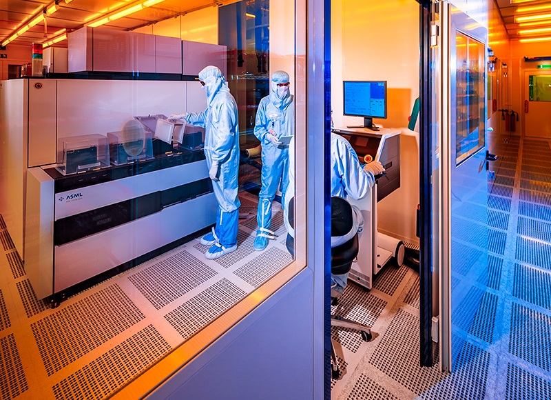
- In-House Characterization & Testing
- Founded
- 2023
- Industries
- Telecommunications, Data centers / AI, Optical communication, Fiber sensing, Satellite communications, Spectroscopy
- 01
Design (in-house R&D)
- 02
Ion implantation of erbium into silicon nitride waveguides
- 03
Wafer-level nanofabrication (monolithic silicon photonics integration)
- 04
Hybrid integration of photonic components
- 05
Optical characterization and testing
- 06
Delivery
Materials & Processes
Silicon nitride
Low-loss waveguide platform, doped via controlled ion implantation for efficient on-chip amplification.
Erbium-doped silicon nitride
Active waveguide material for EDWA amplifiers and EDWL lasers across the C+L bands.
Silicon
Photonics platform for monolithic integration of the amplifiers on a chip.
Sites
Lausanne
CHHeadquarters, R&D and production (access to EPFL nanofabrication CMi)
- Lot size
- Prototype to wafer-level high-volume production
- Materials
- Silicon nitride, erbium, silicon
- Nanofabrication facilities (EPFL CMi)
- Optical test and measurement infrastructure
Components & Products

Inside the production
Industries
Processes & technical limits
| Processes | Tolerance | Max. part | Weight | Lot size | Materials |
|---|---|---|---|---|---|
| Ion implantation of erbium / rare-earth ions into silicon nitride waveguides (EDWA manufacturing)Engineering | – | – | – | – | Silicon nitride, Erbium (rare-earth ions) |
| Wafer-level nanofabrication of photonic integrated circuits (monolithic integration withEngineering | – | – | – | – | Silicon nitride, Silicon |
| Custom design & fabrication using 3D printingAdditive | – | – | – | – | – |
| Custom design & fabrication using CNC machiningMachining | – | – | – | – | – |
| Custom design & fabrication using laser cuttingMachining | – | – | – | – | – |
| Erbium-doped waveguide lasers (EDWL) – manufacturingEngineering | – | – | – | – | Erbium-doped silicon nitride |
| On-chip optical amplifiers (EDWA) – manufacturing (30 dB gain, 300 mW output, NF <5 dB)Engineering | – | – | – | – | Erbium-doped silicon nitride |
| Hybrid integration of photonic productsJoining | – | – | – | – | Silicon |
2 Anlagen & Maschinen
| Machine | Manufacturer / model | Quantity | Working area | Year built | Site |
|---|---|---|---|---|---|
| Nanofabrication facilities (access via EPFL Center of MicroNanoTechnology CMi) | EPFL | – | – | – | EPFL Innovation Park, Lausanne |
| Optical test and measurement infrastructure (characterization) | – | – | – | – | EPFL Innovation Park, Lausanne |
Additional services
Quality
The entire development cycle, including design, fabrication and characterization, is carried out in-house; a dedicated optical test and measurement infrastructure ensures consistent device performance and process control. Certificates are currently not published.
| Evidence | Lausanne |
|---|---|
| In-House Characterization & Testing |
History
- 2023
Founded as a spin-off of the Laboratory of Photonics and Quantum Measurements (LPQM) at EPFL, co-founded by Dr. Amir Youssefi and Prof. Tobias Kippenberg; headquartered in the EPFL Innovation Park, Lausanne.