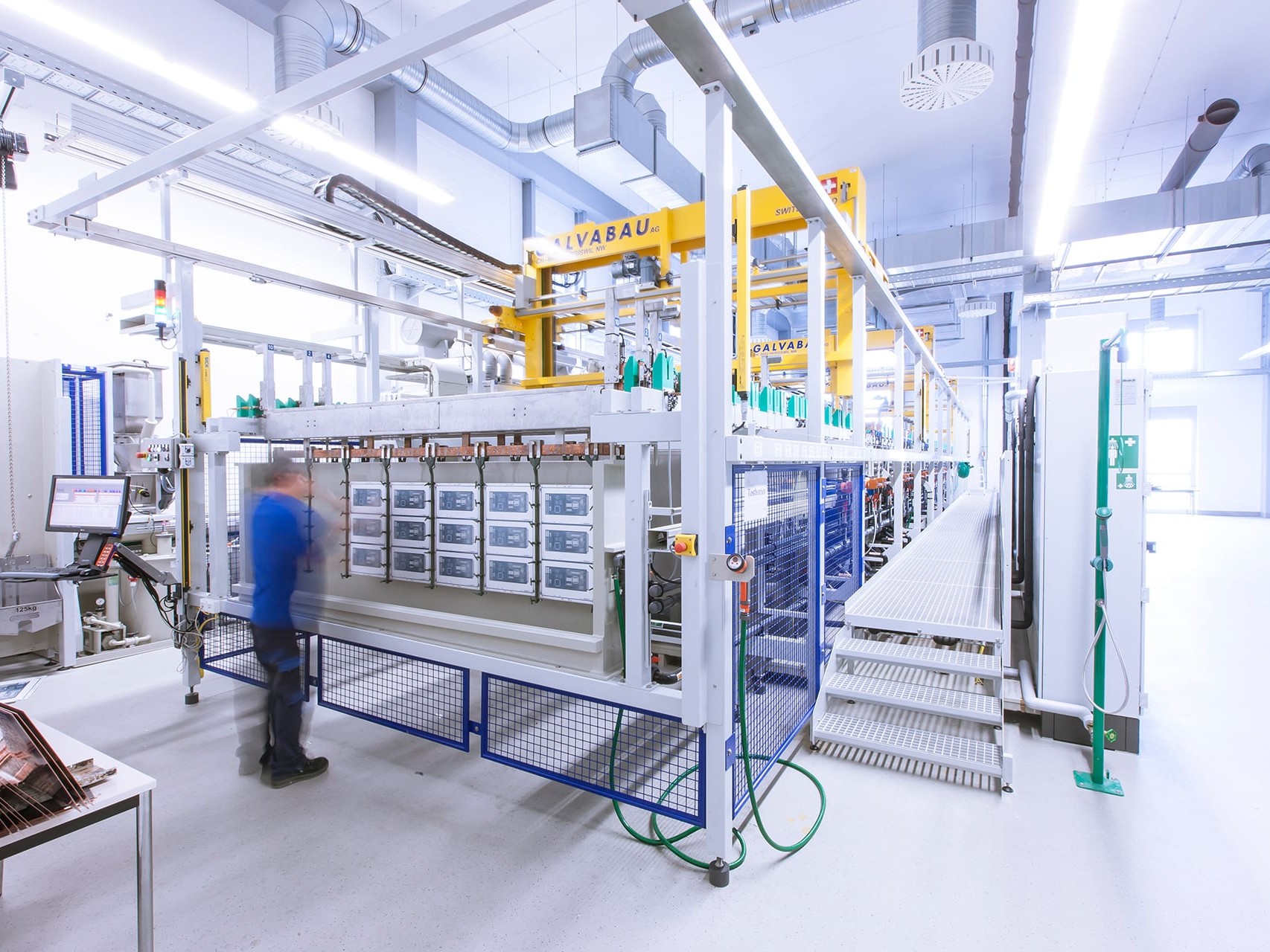
Manufacturer of PCB prototypes and small series – from double-sided boards up to 42-layer multilayers.

Elekonta Marek GmbH & Co. KG
Remseck am Neckar (Stuttgart region)New on Amplifa
About Elekonta Marek
Elekonta Marek GmbH & Co. KG manufactures PCB prototypes and small series for the electronics industry and can look back on more than 50 years of experience in PCB manufacturing. The portfolio includes double-sided plated-through PCBs, multilayers up to 42 layers, flexible and rigid-flex PCBs, RF PCBs made from special materials, heavy copper PCBs and metal-core PCBs (IMS, MCS with copper core); the focus of production is on multilayer manufacturing. Processes used include drilling, direct plating, photo printing, dry film resist, pattern plating, etching, soldermask application, surface finishing and contour machining. Impedance-controlled multilayers are tested and delivered. With its PCB Express Service, the company delivers multilayer PCBs for samples and small series within 48 hours of order receipt; it also offers express service, prototype consulting, workshops and advisory services as a development partner. The site is located in the Stuttgart region.
- Site
- Remseck am Neckar
- Processes
- Double-sided plated-through (PTH) PCBs, Multilayer PCBs up to 42 layers, Impedance-controlled multilayers, HDI SBU multilayers, RF PCBs, Heavy copper PCBs, Flexible PCBs, Rigid-flex PCBs
- Materials
- Copper, RF special materials, FR4
- Certificates
- Testing of impedance-controlled multilayers
- Industries
- Electronics industry
- 01
Prototype consulting
- 02
Drilling
- 03
Direct Plating
- 04
Photo printing / dry film resist
- 05
Pattern Plating
- 06
Etching
- 07
Soldermask application
- 08
Surface finishing
- 09
Contour machining
- 10
Testing
- 11
Shipping
Materials & Processes
Copper
Conductor material, also as heavy copper and metal core (IMS, MCS) for high-power applications.
FR4
Base material for double-sided plated-through PCBs and multilayers.
RF special materials
Special materials for PCBs with high-frequency applications.
Sites
Remseck am Neckar
DEHeadquarters and PCB manufacturing
- Lot size
- Prototypes to small series
- Materials
- Copper, FR4, RF special materials
- PCB Express Service
PCBs
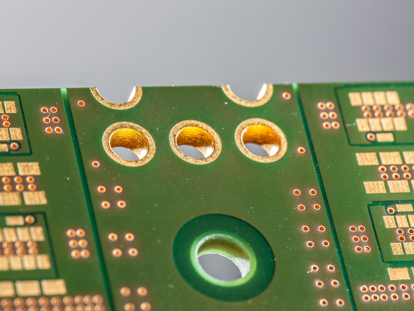
Inside the production

Industries
Processes & technical limits
| Processes | Tolerance | Max. part | Weight | Lot size | Materials |
|---|---|---|---|---|---|
| Double-sided plated-through (PTH) PCBsJoining | – | – | – | Prototypes – Small series | Copper, FR4 |
| Multilayer PCBs up to 42 layersJoining | – | – | – | – | – |
| Impedance-controlled multilayersJoining | – | – | – | – | – |
| HDI SBU multilayersJoining | – | – | – | – | – |
| RF PCBsJoining | – | – | – | – | RF special materials |
| Heavy copper PCBsJoining | – | – | – | – | Copper |
| Flexible PCBsJoining | – | – | – | – | – |
| Rigid-flex PCBsJoining | – | – | – | – | – |
| Metal-core PCBs IMS, MCS (Cu)Joining | – | – | – | – | Copper |
| DrillingMachining | – | – | – | – | – |
| Direct PlatingSurface treatment | – | – | – | – | – |
| Photo printing / dry film resistSurface treatment | – | – | – | – | – |
| Pattern PlatingSurface treatment | – | – | – | – | – |
| EtchingSurface treatment | – | – | – | – | – |
| Soldermask applicationSurface treatment | – | – | – | – | – |
| Surface finishing (PCB surfaces)Surface treatment | – | – | – | – | – |
| Contour machining (PCBs)Machining | – | – | – | – | – |
| Prototype consulting / PCB development partnerEngineering | – | – | – | – | – |
Additional services
Quality
Impedance-controlled multilayers are tested; the company places high demands on quality and adherence to delivery dates.
| Evidence | Remseck am Neckar |
|---|---|
| Testing of impedance-controlled multilayers |
History
Start of PCB manufacturing; over five decades of continuous expansion of the product range and production equipment (more than 50 years of experience)