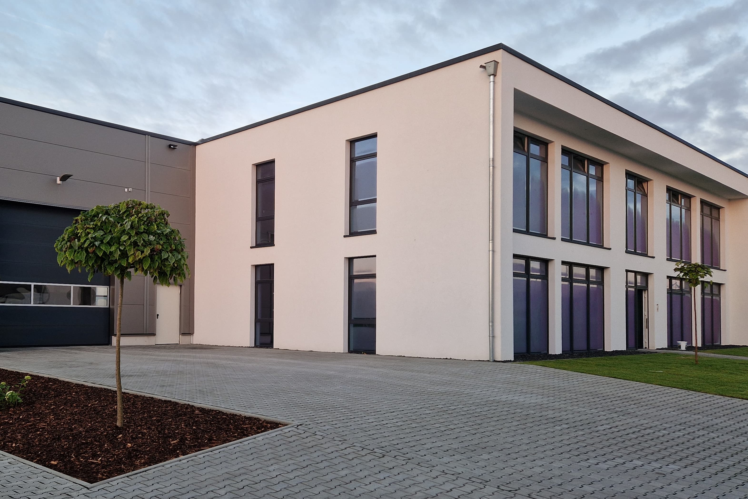
Develops and manufactures epitaxy production systems and monocrystalline templates for wide-bandgap semiconductors
ELEMENT 3-5 GmbH
BaesweilerNew on Amplifa
About ELEMENT 3-5
ELEMENT 3-5 GmbH is a semiconductor company founded in 2010 as a spin-off of RWTH Aachen (predecessor: AIXaTECH GmbH), headquartered in Baesweiler near Aachen. The company develops and manufactures epitaxy production systems based on its own Next Level Epitaxy technology, which deposits monocrystalline layers at process temperatures below 300 °C — with energy savings of up to 90%, up to ten times higher throughput, and without the use of toxic process gases. Core products are the ACCELERATOR 3500K production system for monocrystalline templates for wide-bandgap semiconductors (including LEDs, miniLEDs, microLEDs, HEMTs, power electronics) and the ENABLER 150K system for monocrystalline bulk acoustic wave filters based on AlN and AlScN. In addition to the systems business, ELEMENT 3-5 offers substrate coating in its own technical facility, process development, technology roadmaps, as well as on-site process support and monitoring at the customer's premises. The materials processed are primarily silicon carbide (SiC) and III-V compound semiconductors. With an EU state aid approval of EUR 353 million (2026), the company is building a fab for SiC epiwafers in Baesweiler. The team comprises fewer than 50 employees in Germany; in 2025 the company was named 'Innovator of the Year' (TOP 100, size class A).
- Site
- Baesweiler
- Processes
- Next Level Epitaxy (plasma epitaxy, production of monocrystalline layers/templates), SiC epiwafer production, Deposition of monocrystalline structures at process temperatures below 300 °C, Epitaxy for the production of monocrystalline templates for LEDs, miniLEDs, microLEDs and HEMTs, Epitaxy for the production of monocrystalline bulk acoustic wave filters (BAW filters), Epitaxy with integrated nanostructuring (laser structuring, EPIWIN project), Epitaxy of semiconductor layers (Next Level Epitaxy), Manufacture of monocrystalline templates/epiwafers
- Materials
- Silicon carbide, AlN, AlScN, Wide-bandgap semiconductors (compounds of groups 3 and 5), Wide-bandgap semiconductors (III-V compounds)
- Certificates
- ISO 9001
- Founded
- 2010
- Employees
- < 50 (Germany)
- Industries
- Semiconductor industry, LED / miniLED / microLED displays, Power electronics (SiC power semiconductors), Telecommunications (BAW filters), Lighting
- 01
Requirements analysis and technology roadmap
- 02
Substrate coating in the company's own technical facility
- 03
Characterization and fine-tuning of processes
- 04
Series production of the epitaxy systems
- 05
Commissioning and on-site process support at the customer
- 06
Monitoring of process characteristics and specifications
Materials & Processes
Silicon carbide
Base material for the planned SiC epiwafer fab and power electronics applications.
AlN
Material for monocrystalline bulk acoustic wave filters in the ENABLER 150K system.
AlScN
Alternative filter material choice in the ENABLER 150K for higher telecommunications frequencies.
Wide-bandgap semiconductors (III-V compounds)
Deposition of new material stacks beyond conventional methods thanks to low process temperature.
Sites
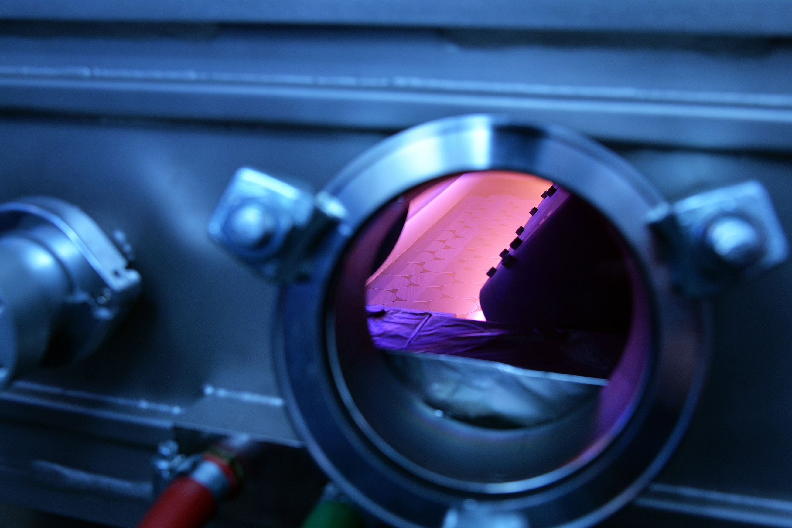
Baesweiler
DEHeadquarters, technical facility and production
- Lot size
- Prototype to series (epitaxy systems)
- Materials
- SiC, AlN, AlScN, III-V semiconductors
- ACCELERATOR 3500K epitaxy production system
- ENABLER 150K epitaxy system for BAW filters
Systems & Components

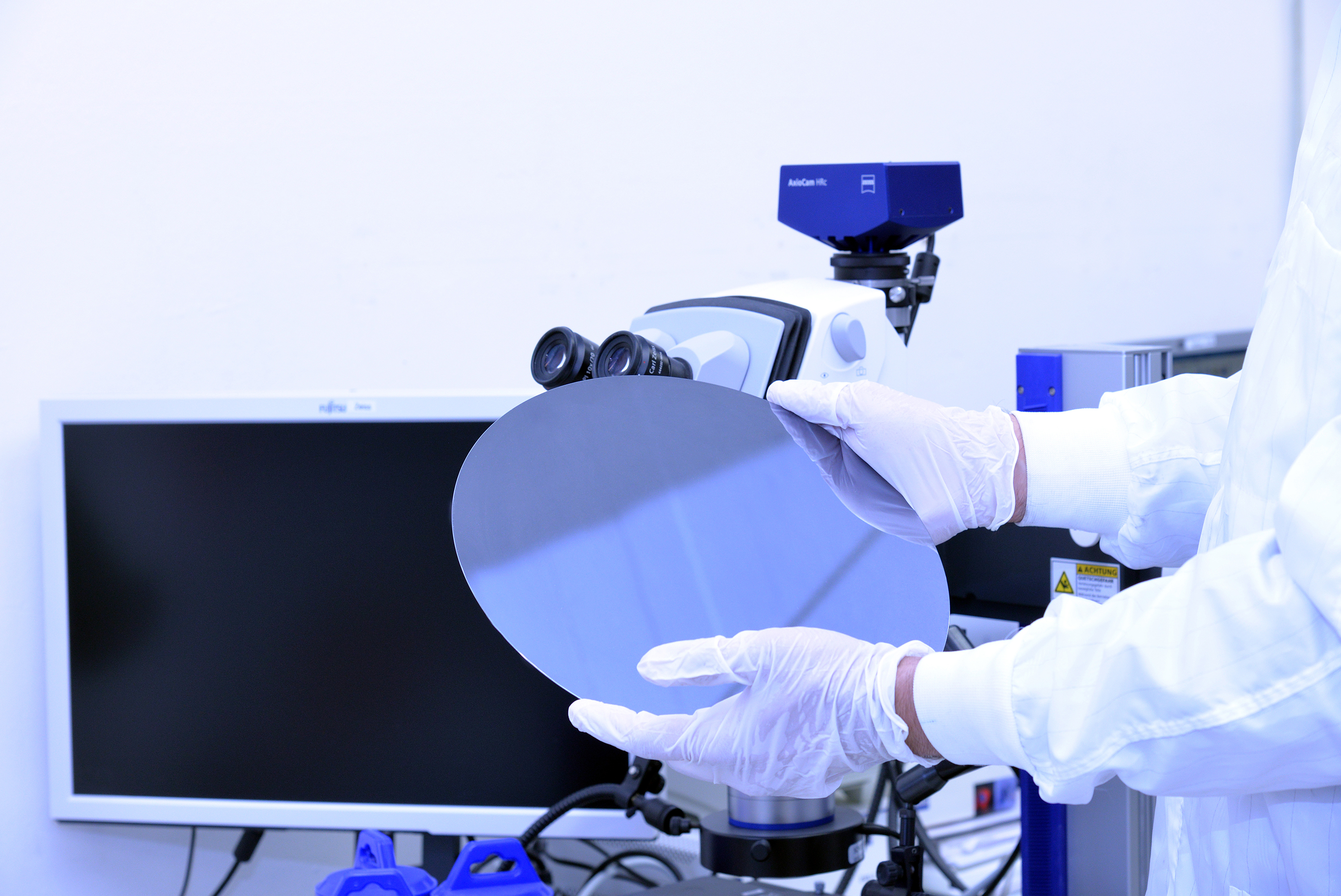
Inside the production
Industries
Processes & technical limits
| Processes | Tolerance | Max. part | Weight | Lot size | Materials |
|---|---|---|---|---|---|
| Next Level Epitaxy (plasma epitaxy, production of monocrystalline layers/templates)Coating/Semiconductor manufacturing | – | – | – | – | Silicon carbide (SiC), Wide-bandgap semiconductors, Compounds of groups 3 and 5 (III-V), temperature-sensitive substrates |
| SiC epiwafer productionCoating/Semiconductor manufacturing | – | – | – | – | Silicon carbide (SiC) |
| Deposition of monocrystalline structures at process temperatures below 300 °CCoating/Semiconductor manufacturing | – | – | – | – | III-V compound semiconductors, Wide-bandgap semiconductors |
| Epitaxy for the production of monocrystalline templates for LEDs, miniLEDs, microLEDs and HEMTsCoating/Semiconductor manufacturing | – | – | – | – | Wide-bandgap semiconductors, III-V compound semiconductors |
| Epitaxy for the production of monocrystalline bulk acoustic wave filters (BAW filters)Coating/Semiconductor manufacturing | – | – | – | – | AlN, AlScN |
| Epitaxy with integrated nanostructuring (laser structuring, EPIWIN project)Coating/Semiconductor manufacturing | – | – | – | – | Wide-bandgap semiconductors |
2 Anlagen & Maschinen
| Machine | Manufacturer / model | Quantity | Working area | Year built | Site |
|---|---|---|---|---|---|
| Epitaxy production system (Next Level Epitaxy, plasma technology) | ELEMENT 3-5 GmbH ACCELERATOR 3500K | – | – | – | Baesweiler |
| Epitaxy system for monocrystalline bulk acoustic wave filters | ELEMENT 3-5 GmbH ENABLER 150K | – | – | – | Baesweiler |
Additional services
Reference customers
Quality
Process characteristics and specifications are monitored through characterization and continuous monitoring; the vertical alignment of the substrates enables particle-free deposition with high homogeneity and reproducibility.
| Evidence | Baesweiler |
|---|---|
| ISO 9001 |
History
- 2010
Founded as AIXaTECH GmbH as a spin-off of RWTH Aachen by Dr. Yilmaz Dikme and others
- 2015
Independent validation of the technology by Dr. Yilmaz Dikme and Dr. Volker Sinhoff; Volker Sinhoff takes over as Managing Director
- 2022
Series A financing (led by AVV Investment GmbH, amount in the tens of millions); Ghassan Barbar takes over product management/sales for the ACCELERATOR 3500K
- 2022
Move into the new headquarters building, Robert-Koch-Str. 6a, 52499 Baesweiler (ready for occupancy on 1 October)
- 2024
Funding approval for the GREEN EPITAXY lighthouse project in the Rhenish mining region
- 2025
Market entry with the first ACCELERATOR 3500K systems at pilot customers; award 'Innovator of the Year' (TOP 100, size class A) on 27 June
- 2025
Exhibition at the NRW Nano Conference in Dortmund (30.09.–01.10.)
- 2026
EU Commission approves EUR 353 million in state aid for a SiC epiwafer fab in Baesweiler
- 2026
Visit by NRW Minister of Economic Affairs Mona Neubaur in Baesweiler as part of the summer tour