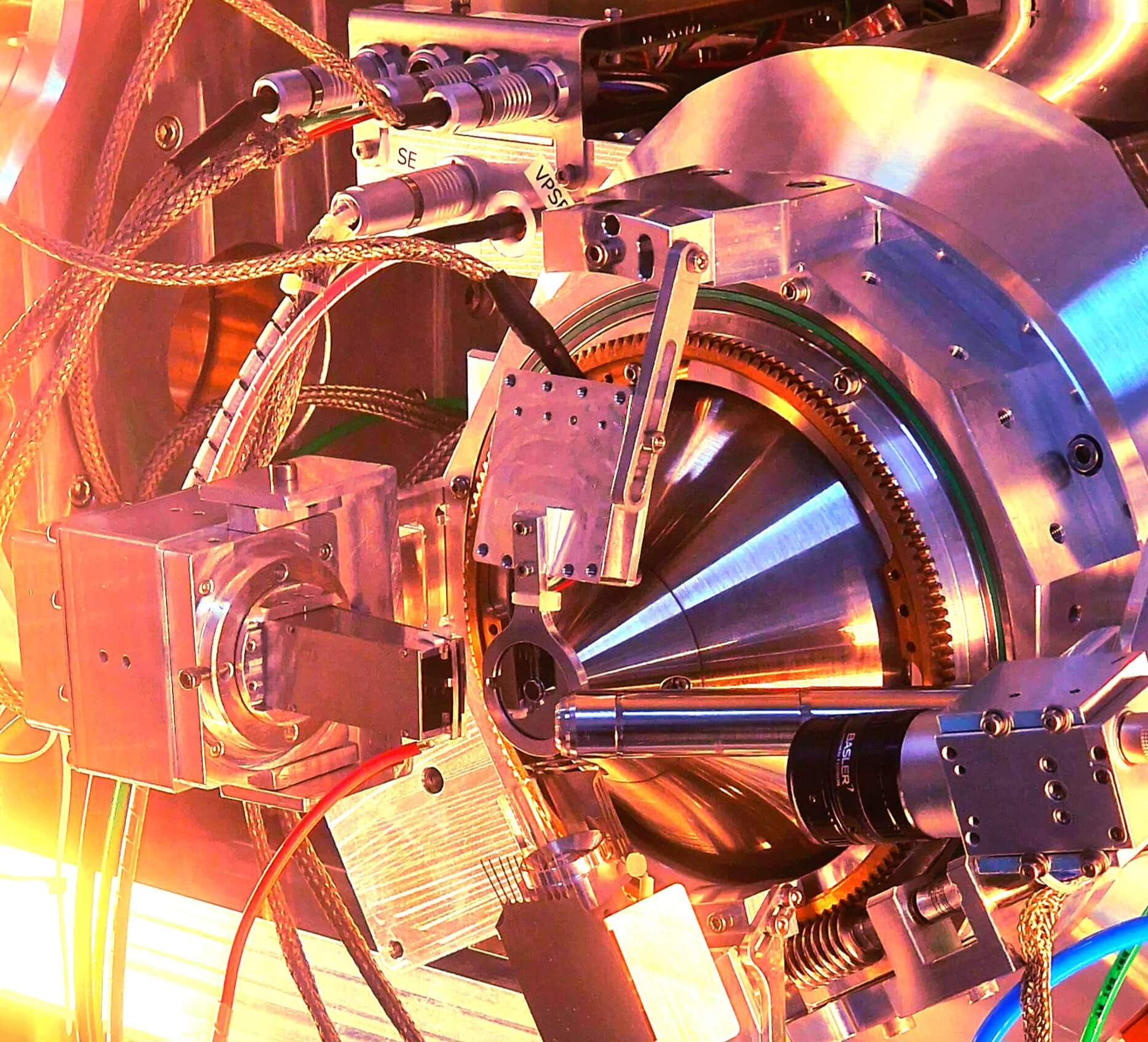
Manufacturer of the MIRA Large-Chamber Scanning Electron Microscope for non-destructive testing of large components

ELLCIE Industries GmbH
Grevesmühlen · GermanyNew on Amplifa
About ELLCIE Industries
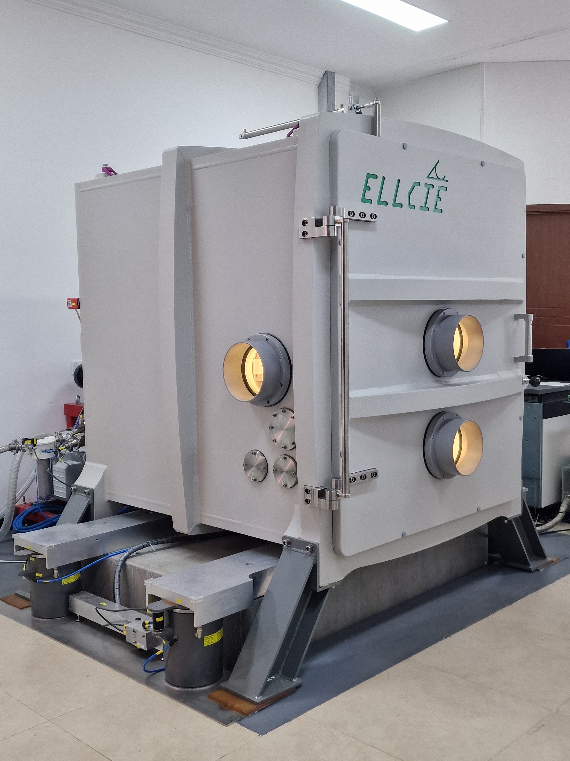
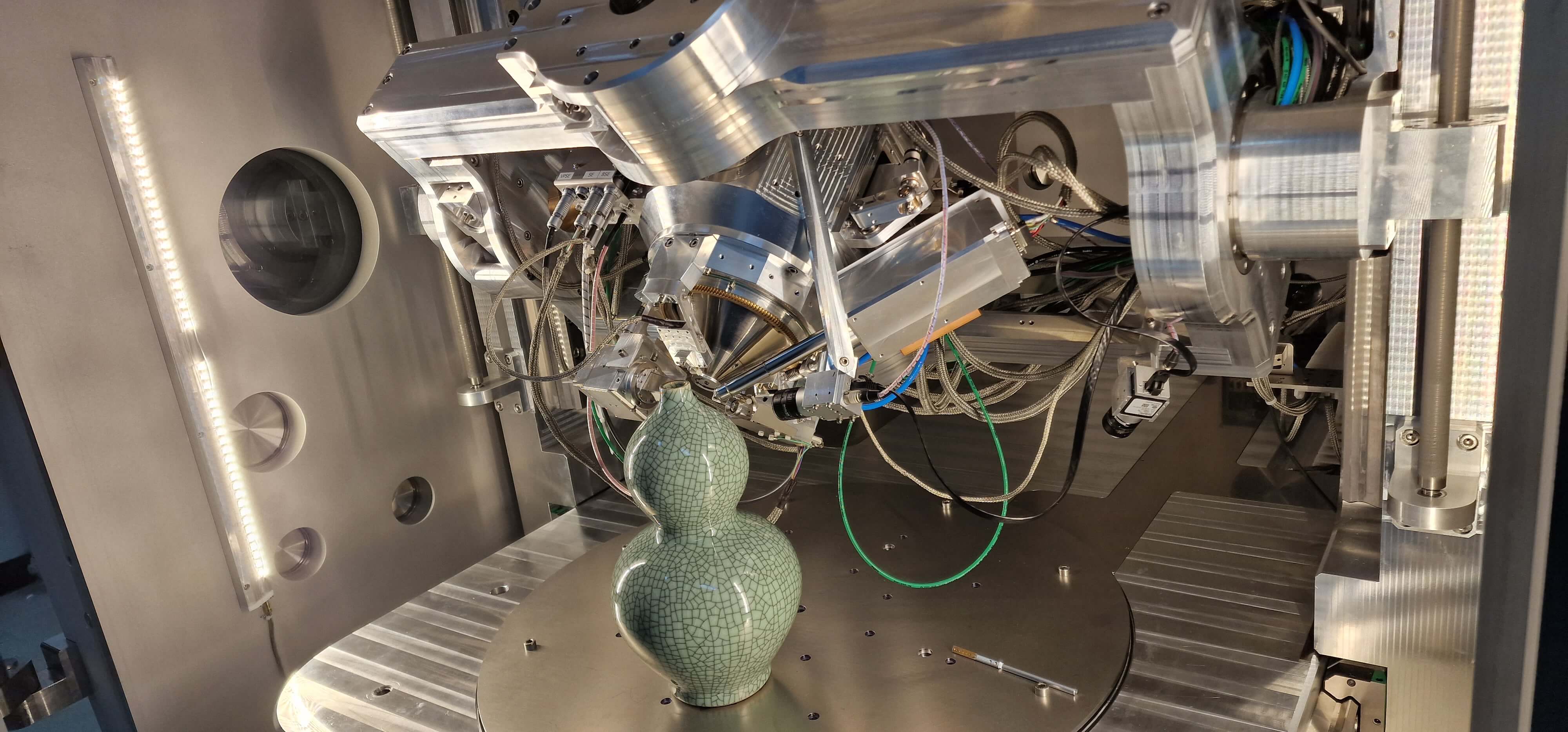
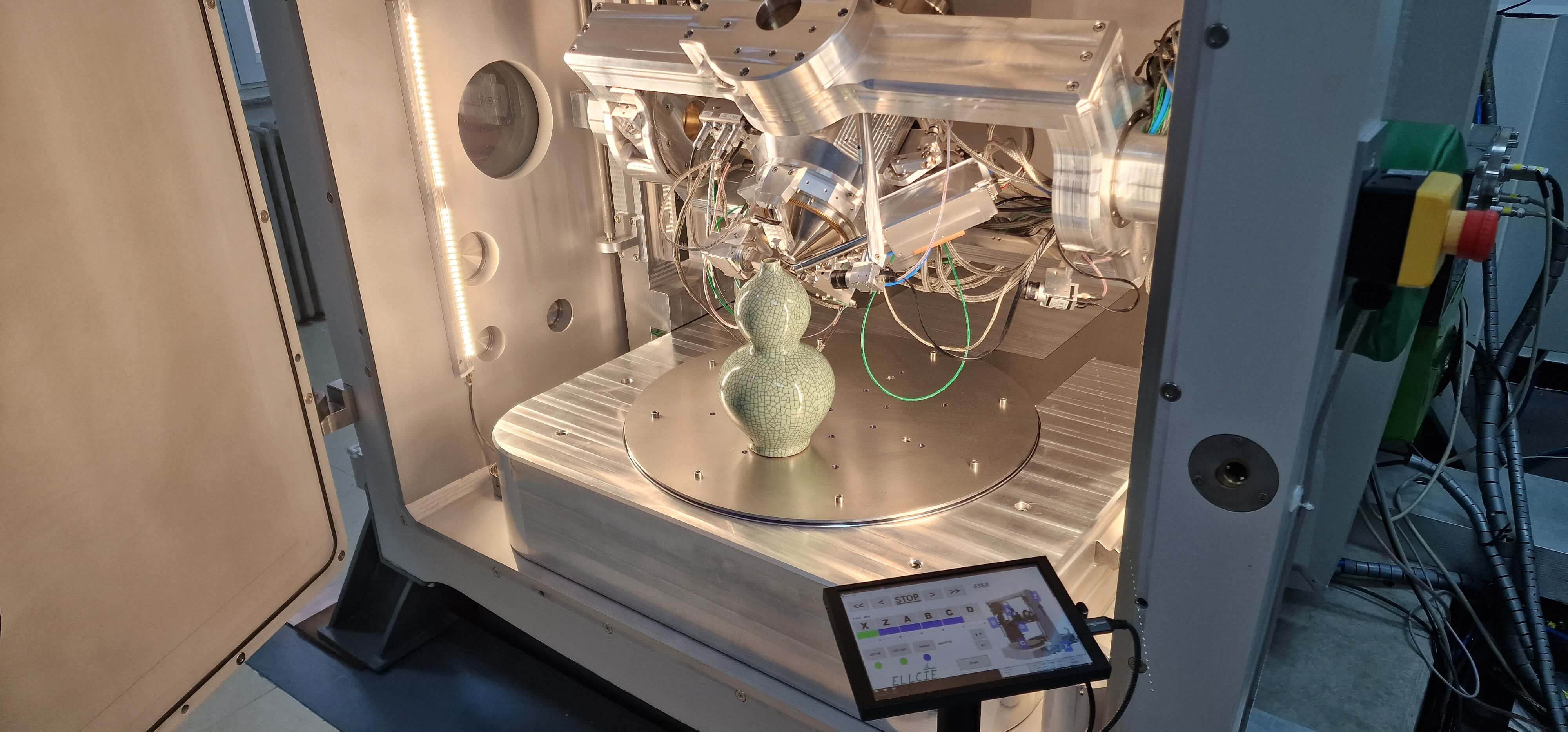
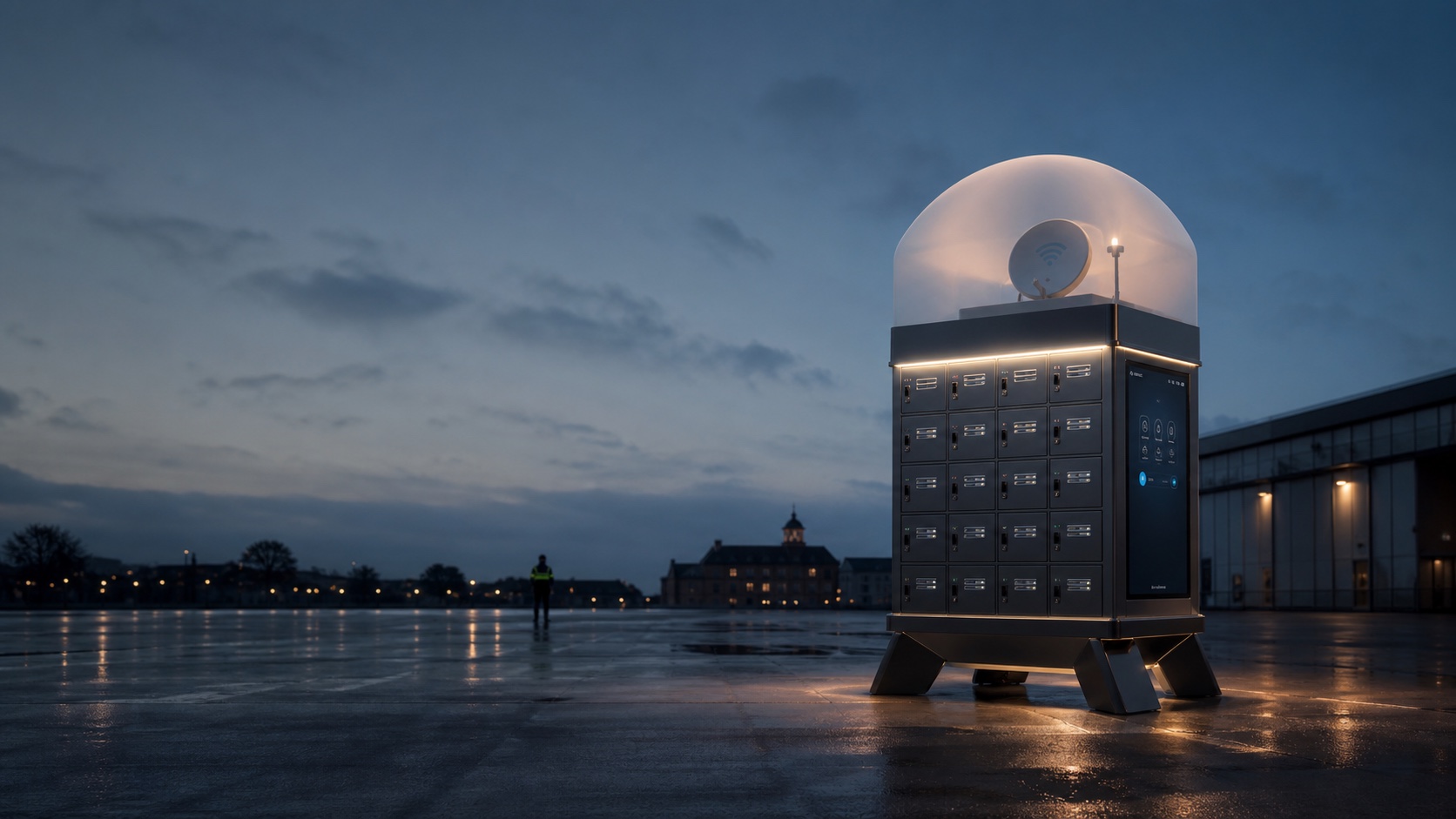
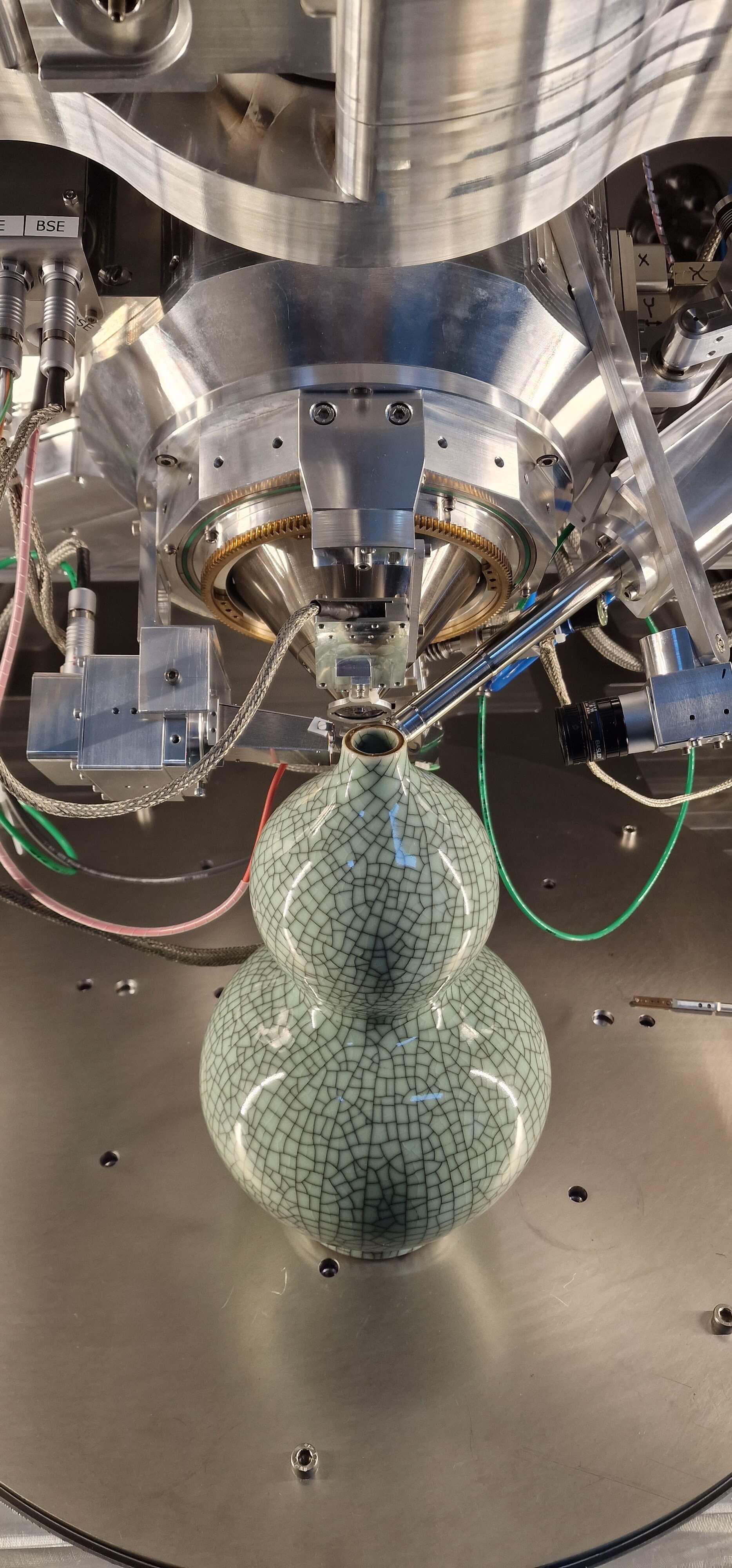
ELLCIE Industries GmbH, headquartered in Grevesmühlen, develops and manufactures the Large Chamber Scanning Electron Microscope (LC-SEM) MIRA, a scanning electron microscope with a bell-type chamber for non-destructive testing (NDT) and material analysis of very large samples. The system enables direct examination of intact components up to 1500 mm in diameter and 300 kg in mass without destructive sampling or disassembly. Core features include a patented 5+1-axis positioning system, a resolution below 10 nm, integrated EDS and EBSD analytics, as well as optional FIB, FT-IR and camera systems. A special feature is the ability to perform fatigue testing in-situ inside the vacuum chamber. In addition to its microscopy division, ELLCIE develops with Conterbase mobile infrastructure for disaster relief, providing power, satellite communication, digital signage, lighting and charging infrastructure. Customer industries include aerospace, defense, automotive, materials science, electronics, medical technology, forensics, cultural heritage conservation as well as authorities and relief organizations.
- Site
- Grevesmühlen
- Processes
- Scanning electron microscopy (LC-SEM) / material analysis incl. EDS, EBSD, optional FIB, FT-IR,, Non-destructive testing (NDT), In-situ analysis including fatigue tests in the SEM, EDS and EBSD analytics, Optional FIB, FT-IR and camera systems, Large-component inspection up to 1500 mm diameter / 300 kg, Failure analysis, 3D print model (STL) of the MIRA system
- Materials
- Large Chamber Scanning Electron Microscopy, Energy Dispersive X-Ray Spectroscopy, Electron Backscatter Diffraction, In-situ fatigue testing, Focused Ion Beam (optional), Fourier-Transform Infrared Spectroscopy (optional)
- Certificates
- Resolution <10 nm at 300,000x magnification, Positioning repeatability ±50 µm, Active vibration damping system
- Industries
- Aerospace, Defense technology, Automotive, Materials science and research, Electronics/semiconductors, Medical technology
- 01
Engineering and design of the LC-SEM
- 02
Manufacturing and system integration of the vacuum chamber
- 03
Installation and commissioning at the customer's site
- 04
Analytical services (EDS, EBSD, in-situ tests)
- 05
Service and expansion through optional modules
Processes and Analytics
Large Chamber Scanning Electron Microscopy
Non-destructive imaging and analysis of large components up to 1500 mm and 300 kg with resolution below 10 nm.
Energy Dispersive X-Ray Spectroscopy
Elemental analysis for material identification directly at the sample position.
Electron Backscatter Diffraction
Analysis of crystal orientations and microstructures, phase transformations and microstructure.
In-situ fatigue testing
Fatigue and deformation tests inside the vacuum chamber to observe crack initiation and propagation.
Focused Ion Beam (optional)
Optional module for local material removal and cross-section analysis.
Fourier-Transform Infrared Spectroscopy (optional)
Optional IR analysis for chemical characterization of sensitive materials.
Locations
Grevesmühlen
DEProduction site / Company headquarters
- Part weight / size
- Samples up to 1500 mm diameter, 1500 mm height, 300 kg
- Materials
- Metals, composites, electronics, biomaterials, artifacts
- MIRA LC-SEM (chamber 3/9/12 m³)
- 5+1-axis positioning system
- EDS/EBSD detectors
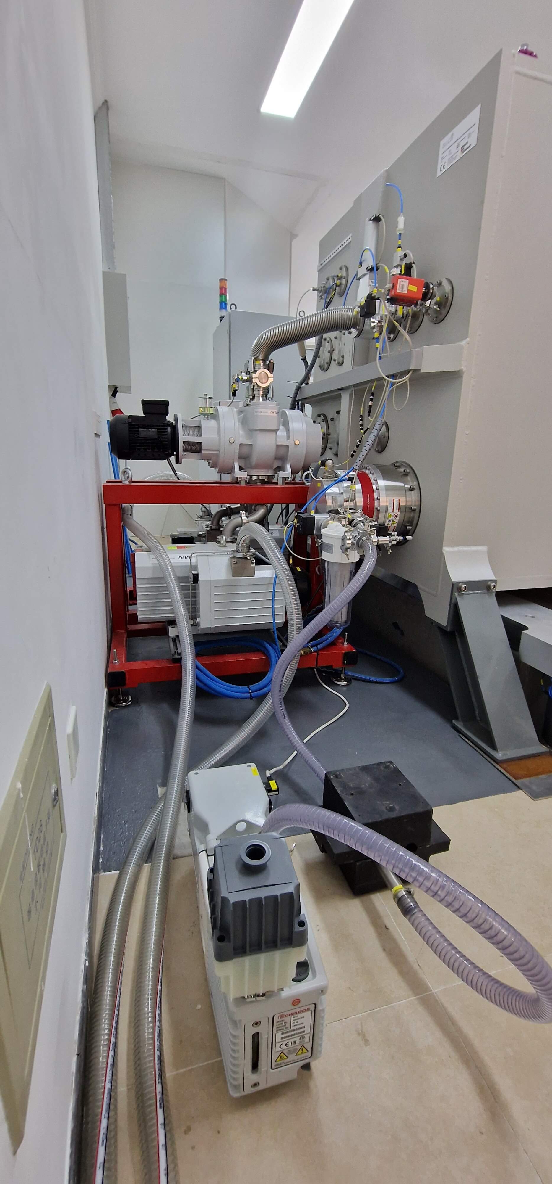
- Turbomolecular pump 2400 l/s
- Rotary vane / rotary piston pump
Components and Systems
Inside the production
Industries
Processes & technical limits
| Processes | Tolerance | Max. part | Weight | Lot size | Materials |
|---|---|---|---|---|---|
| Scanning electron microscopy (LC-SEM) / material analysis incl. EDS, EBSD, optional FIB, FT-IR,Testing | ±50 µm (positioning repeatability) | 1500 mm × 1500 mm diameter × 1500 mm | 300 kg | – | – |
1 Anlagen & Maschinen
| Machine | Manufacturer / model | Quantity | Working area | Year built | Site |
|---|---|---|---|---|---|
| Large Chamber Scanning Electron Microscope (LC-SEM) | ELLCIE Industries MIRA | – | Samples up to 1500 mm diameter, 1500 mm height; chamber 3/9/12 m³; 5+1 axes (X 600/1000/1500 mm, Z | – | Grevesmühlen, Germany |
Additional services
Quality and Precision
The MIRA system achieves a positioning repeatability of ±50 µm and a resolution below 10 nm over an acceleration voltage range of 0.2–30 keV; an active vibration damping system ensures stable imaging conditions.
| Evidence | Grevesmühlen |
|---|---|
| Resolution <10 nm at 300,000x magnification | |
| Positioning repeatability ±50 µm | |
| Active vibration damping system |
History
Founded by Dipl.-Ing. Martin Klein; specialization in large-chamber scanning electron microscopy for space and defense applications.