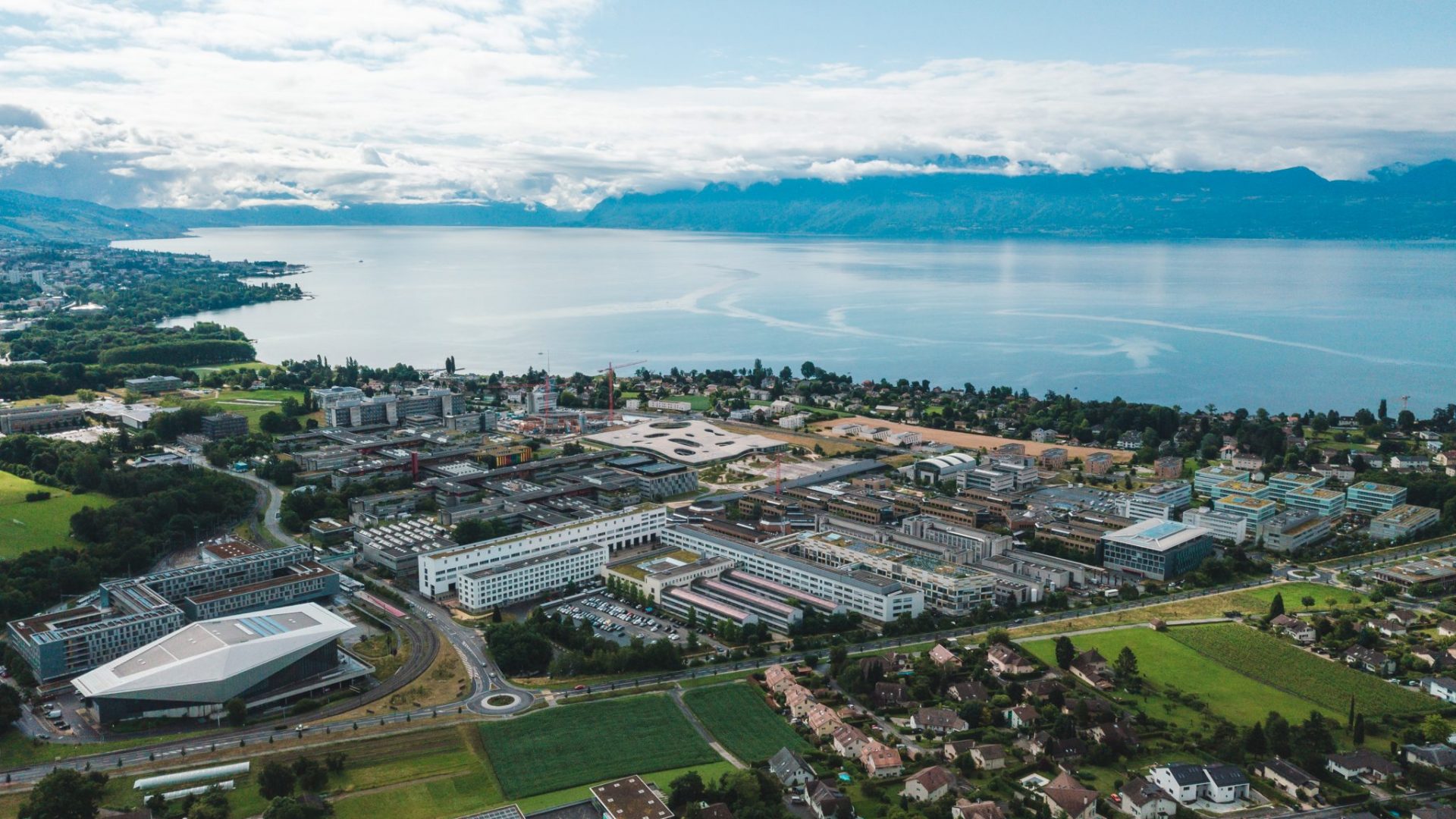
Federal technical university with CMi cleanroom and M2C infrastructure for micro-/nano-fabrication, 3D metal printing and characterization

EPFL - École polytechnique fédérale de Lausanne
Lausanne (CH-1015) · Neuchâtel (CH-2000)New on Amplifa
About EPFL
EPFL is a public technical university of the ETH Domain in Switzerland, based in Lausanne with approximately 6,500 employees. In addition to its three missions of teaching, research and innovation, EPFL operates research and manufacturing infrastructure that is also accessible to external partners. The Center of MicroNanoTechnology (CMi) provides a cleanroom with lithography (electron beam and photolithography), plasma and ion beam etching, thin-film processes (LPCVD, oxidation, ALD, PECVD, sputtering) as well as comprehensive metrology (SEM/FIB, AFM, stylus profilometry) for wafers up to 150 mm. The M2C center (Advanced Manufacturing) offers 3D metal printing using the laser powder bed fusion process, metal powder atomization, femtosecond laser processing and X-ray tomography. At the Associated Campus Neuchâtel (Microcity), shared laboratories for microscopy, optical spectroscopy, electrical characterization, chemistry and probe station measurements are available. Companies can collaborate with EPFL through shared equipment access, technology transfer and internship programs.
- Site
- CH-1015 Lausanne
- Processes
- Electron beam lithography (Raith EBPG5000+/EBPG5200+), Photolithography (EVG 150, Süss ACS200 Gen3, mask aligner, laser writer, DUV stepper), Ion Beam Etching (Veeco Nexus IBE350), LPCVD / oxidation / diffusion / doping / annealing (Centrotherm furnaces), Atomic Layer Deposition ALD (BENEQ TFS200), Rapid Thermal Processing (JETFIRST 200), Flash Lamp Annealing (ROVAK Semi-Line 3.0), Thin-film deposition PECVD / sputtering
- Materials
- Silicon / polysilicon / amorphous silicon, Silicon dioxide (LTO, TEOS, HTO, PSG, BPSG, BSG), Silicon nitride / low-stress silicon nitride, Aluminum oxide (ALD), Titanium dioxide (ALD), Hafnium dioxide (ALD), Platinum (ALD), Gallium arsenide
- Certificates
- Cleanroom metrology (AFM, SEM/FIB, EDX, profilometry), Optical spectroscopy (Raman, UV-Vis, FTIR, ellipsometry), Electrical characterization / probe station, Mechanical characterization (vibration testing up to 200g)
- Employees
- 6500
- Industries
- Higher education, Research and development, Innovation / technology transfer, Micro- and nanotechnology, Additive manufacturing, Micro- and nanotechnology (CMi)
- 01
Process development and consulting
- 02
Lithography (electron beam / photolithography)
- 03
Thin-film deposition (LPCVD, oxidation, ALD, PECVD, sputtering)
- 04
Etching (plasma, ion beam, wet etching)
- 05
3D metal additive manufacturing and powder production (M2C)
- 06
Metrology and characterization
- 07
Technology transfer and continuing education
Materials and Processes
Silicon / polysilicon / amorphous silicon
Base material for LPCVD, oxidation, diffusion, plasma etching and electron beam lithography.
Silicon dioxide (LTO, TEOS, HTO, PSG, BPSG, BSG)
Thin-film material for insulation, masking and etch stop layers.
Silicon nitride / low-stress silicon nitride
LPCVD and plasma etching processes for passivation and MEMS membranes.
Aluminum oxide (ALD)
Deposited by Atomic Layer Deposition at 80–300 °C.
Titanium dioxide (ALD)
Deposited by Atomic Layer Deposition.
Hafnium dioxide (ALD)
High-k dielectric deposited by Atomic Layer Deposition.
Platinum (ALD)
Metal layer deposited by thermal or plasma-enhanced ALD.
Gallium arsenide
Substrate material, among others, for surface metrology.
Silicon carbide
Substrate material for surface metrology.
Sapphire (Al2O3)
Transparent substrate for electron beam lithography.
Aluminum
Alloying of silicon-aluminum compounds in a furnace process.
Metal powder (3D printing)
Feedstock material for laser powder bed fusion and powder atomization at the M2C.
Sites
Lausanne
CHMain campus: teaching, research, innovation, CMi cleanroom, CIME, M2C
- Part weight / size
- Wafers up to 150 mm (lithography)
- Lot size
- Prototypes to research series
- Materials
- Silicon, SiO2, Si3N4, ALD oxides, metals, metal powders
- Raith EBPG5000+ and EBPG5200 plus e-beam lithography (100 keV)
- SPTS Rapier DSE, Alcatel AMS 200 SE, SPTS Synapse/APS, TEL Unity Me (plasma etching)
- Veeco Nexus IBE350 Ion Beam Etcher
- Centrotherm furnaces (15 tubes: LPCVD, oxidation, diffusion)
- BENEQ TFS200 ALD (2 systems)
- EVG 150 and Süss MicroTec ACS200 Gen3 resist clusters
- Zeiss MERLIN, Crossbeam 550/540, Helios G4 PFIB UXe (SEM/FIB)
- Park Systems FX200, Bruker FastScan AFM
- Tencor P-17 Stylus Profiler
- Sisma and EOS 3D metal printers (LPBF)
- Metal Powder Atomizer
- Femtosecond laser source
- X-ray tomography system
Neuchâtel
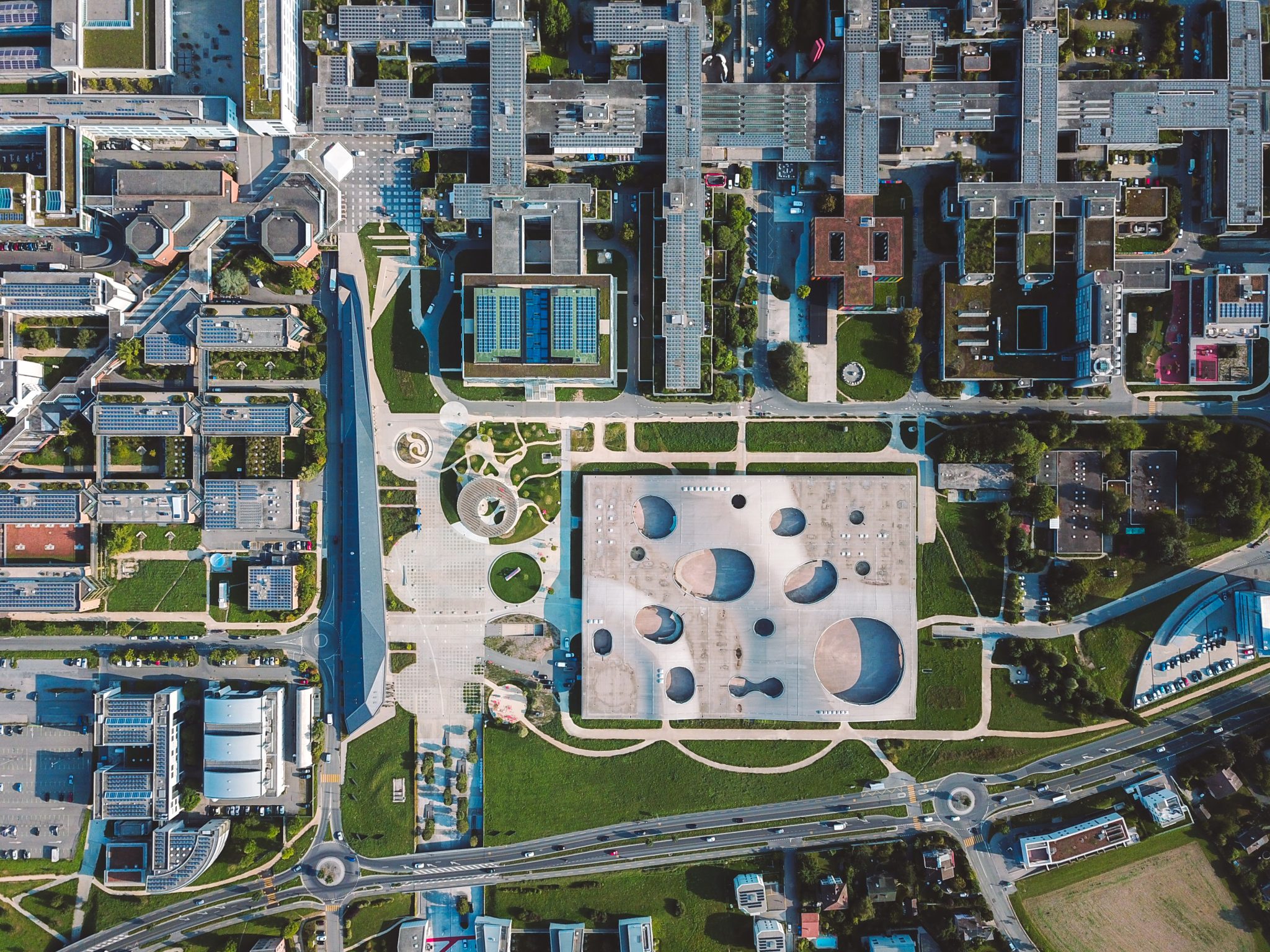
CHAssociated Campus Microcity: shared laboratories (microscopy, spectroscopy, chemistry, bio, probe station)
- Part weight / size
- Samples up to 4" wafer (SEM)
- Lot size
- On request / reservation system
- Materials
- Silicon-based materials, various sputtering materials
- Zeiss SEM Gemini 2 and JEOL JSM-7500 TFE
- Keyence VK X-1000 laser confocal microscope
- Hirox KH-8700 digital microscope
- Lyncee Tec Digital Holographic Microscope
- PECVD/sputter coating systems (PVLAB)
- Raman, UV-Vis, FTIR spectrometers, ellipsometer
- Electromagnetic shaker (up to 200g, 1 Hz–10 kHz)
- Probe station
- Chemistry laboratory with galvanostat and analysis instruments
Inside the production


Industries
Processes & technical limits
| Processes | Tolerance | Max. part | Weight | Lot size | Materials |
|---|---|---|---|---|---|
| Electron beam lithography (Raith EBPG5000+/EBPG5200+)Testing | – | 150 mm wafer | – | – | Silicon wafers, Glass, Sapphire, CaF2, Diamond, Lithium niobate, SiO2, Si3N4 |
| Photolithography (EVG 150, Süss ACS200 Gen3, mask aligner, laser writer, DUV stepper)Testing | Overlay >20 nm (ebeam) | 150 mm wafer | – | – | Silicon, SiO2, Si3N4, Photoresist (AZ ECI 3007, AZ 3027, AZ nLOF), LOR, BARC |
| Ion Beam Etching (Veeco Nexus IBE350)Surface | – | 100 mm wafer, max 4 mm thick | – | – | Any materials (pure physical sputtering) |
| Surface | – | 100 mm wafer | – | – | Silicon, SOI, SiO2, Si3N4, Glass |
| LPCVD / oxidation / diffusion / doping / annealing (Centrotherm furnaces)Heat treatment | – | – | – | – | Silicon, Polysilicon, Amorphous silicon, Si3N4, SixNy, LTO, PSG, BPSG, BSG, TEOS, HTO, Aluminum (alloying), Phosphorus doping |
| Atomic Layer Deposition ALD (BENEQ TFS200)Surface | – | – | – | – | Al2O3, TiO2, HfO2, SiO2, Pt |
| Rapid Thermal Processing (JETFIRST 200)Heat treatment | – | 8" wafer | – | – | Silicon |
| Flash Lamp Annealing (ROVAK Semi-Line 3.0)Heat treatment | – | 4" wafer, max 2 mm thick | – | – | Silicon |
| Thin-film deposition PECVD / sputteringSurface | – | – | – | – | Silicon-based materials, Various materials (sputtering) |
| Laser Powder Bed Fusion 3D Metal Printing (Sisma, EOS)Additive | – | – | – | – | Metal powder |
| Metal powder atomizationAdditive | – | – | – | – | Metal |
| Femtosecond laser processingSurface | – | – | – | – | – |
| Nanoimprint lithographyTesting | – | – | – | – | – |
| Mechanical characterization (vibration/shaker testing up to 200g, 1 Hz–10 kHz)Testing | – | – | – | – | – |
| Wet etching (KOH, BHF, Piranha)Surface | – | – | – | – | Silicon, Si3N4, SiO2 |
| Surface metrology / stylus profiling (Tencor P-17)Testing | RMS roughness measurable | 200 mm scan length × 200 mm × 1 mm vertical range | – | – | AlTiC, GaAs, Si, SiC, Sapphire |
43 Anlagen & Maschinen
| Machine | Manufacturer / model | Quantity | Working area | Year built | Site |
|---|---|---|---|---|---|
| Electron beam lithography system | Raith EBPG5000+ | 1 | 50/100/150 mm wafer | – | CMi Zone 7, Lausanne |
| Electron beam lithography system | Raith EBPG5200 plus | 1 | 50/100/150 mm wafer | – | CMi Zone 1, Lausanne |
| Ion Beam Etcher | Veeco Nexus IBE350 | 1 | 100 mm wafer (max 4 mm thick), 350 mm Ar broad beam | – | CMi Zone 11 |
| ICP Dry Etcher (deep Si etching) | SPTS Rapier DSE | 1 | 100 mm wafer | – | CMi Zone 2 |
| ICP Dry Etcher | Alcatel AMS 200 SE | 1 | 100 mm wafer (max 4.5 mm thick) | – | CMi Zone 2 |
| Dielectric Etcher | SPTS Synapse | 1 | 100 mm wafer | – | CMi Zone 2 |
| Dielectric Etcher | SPTS APS | 1 | 100 mm wafer | – | CMi Zone 2 |
| RIE Dry Etcher | TEL Unity Me | 1 | 100 mm wafer | – | CMi |
| LPCVD/oxidation/diffusion furnaces | Centrotherm | 15 | 15 tubes (LPCVD, oxidation, diffusion, alloying, POCl3) | – | CMi Zone 3 |
| Rapid Thermal Processing | JETFIRST 200 | 1 | Dies up to 8" wafer, 200–1100°C | – | CMi Zone 3 |
| Flash Lamp Annealing System | ROVAK Semi-Line 3.0 | 1 | 4" wafer (max 2 mm thick) | – | CMi Zone 8 |
| Atomic Layer Deposition | BENEQ TFS200 (ALD I & II) | 2 | 80–300°C | – | CMi Zone 4 |
| Automated resist processing cluster | EVG 150 | 1 | 100/150 mm wafer (200–750 µm thick) | – | CMi Zone 6 |
| Automated resist processing cluster | Süss MicroTec ACS200 Gen3 | 1 | 100/150 mm wafer | – | CMi Zone 1 |
| Mask processing (Cr blanks) | Hamatech HMR900 | 1 | 4–7 inch masks | – | CMi Zone 6 |
| Spin coater (e-beam resists) | Sawatec SM-150 | 1 | 50/100/150 mm wafer | – | CMi Zone 7 |
| Spin coater with hotplates | Sawatec SM-200 | 1 | – | – | CMi |
| Atomic Force Microscope | Park Systems FX200 | 1 | Up to 200 mm wafer, XY scan 100x100 µm, Z 15 µm | – | CMi Zone 15 |
| Atomic Force Microscope | Bruker FastScan (Icon) | 1 | 150 x 180 mm | – | CMi Zone 20 |
| SEM/plasma FIB | Zeiss/Thermo Fisher Helios G4 PFIB UXe | 1 | 100/150 mm wafer | – | MXC 036 (CIME) |
| SEM/FIB CrossBeam | Zeiss CrossBeam 540 | 1 | 100 mm wafer | – | MXC 039 (CIME) |
| SEM (field-emission scanning electron microscope) | Zeiss MERLIN | 1 | 100 mm wafer, <1 nm resolution | – | CMi Zone 15 |
| SEM CrossBeam | Zeiss Crossbeam 550 | 1 | Up to 8" wafer, 6 & 5 inch masks | – | CMi Zone 15 |
| Stylus Profiler | Tencor (KLA) P-17 | 1 | 200 mm scan stage | – | CMi |
| 3D metal printer (laser powder bed fusion) | Sisma | 1 | – | – | M2C, EPFL |
| 3D metal printer (laser powder bed fusion) | EOS | 1 | – | – | M2C, EPFL |
| Metal powder atomizer | – | 1 | – | – | M2C, EPFL |
| Femtosecond laser source | – | 1 | – | – | M2C, EPFL |
| High resolution X-ray tomography system | – | 1 | – | – | M2C, EPFL |
| Automated pick & place system | – | 1 | – | – | M2C, EPFL |
| Scanning electron microscope | Zeiss Gemini 2 SEM | 1 | 1 nm resolution, 0.02–30 keV | – | Neuchâtel Campus MC B4 202 |
| Scanning electron microscope | JEOL JSM-7500 TFE | 1 | Max 4" wafer | – | Neuchâtel Campus MC B4 204 |
| Laser confocal microscope | Keyence VK X-1000 | 1 | – | – | Neuchâtel Campus MC B4 202 |
| Digital microscope | Hirox KH-8700 | 1 | 35–2500x zoom | – | Neuchâtel Campus MC B4 204 |
| Digital holographic microscope | Lyncee Tec | 1 | MEMS motion up to 20 MHz | – | Neuchâtel Campus |
| PECVD coating system | – | – | Silicon-based materials | – | Neuchâtel Campus MC B1 132 (PVLAB) |
| Electromagnetic shaker (vibration generator) | – | 1 | Up to 200g, 1 Hz–10 kHz | – | Neuchâtel Campus (LMTS) |
| Probe station | – | 1 | – | – | Neuchâtel Campus MC B4 196 |
| Confocal Raman/photoluminescence microscope | – | 1 | Samples up to 10x10 cm | – | Neuchâtel Campus MC A2 285 (PVLAB) |
| UV-Vis spectrometer | – | 1 | 280–25000 nm, samples up to 10x10 cm | – | Neuchâtel Campus MC A2 163 |
| FTIR spectrometer | – | 1 | 400–20000 cm-1, samples up to 5x5 cm | – | Neuchâtel Campus MC A2 284 |
| Ellipsometer | – | 1 | 0.6–6 eV, samples up to 20x20 cm | – | Neuchâtel Campus MC B2 272 |
| Spin coater for polymers with hotplates | Sawatec | 1 | – | – | CMi Zone 13 |
Additional services
Characterization and Metrology
Process control is carried out via integrated metrology in the CMi cleanroom: AFM (Park Systems FX200, Bruker FastScan), SEM/FIB (Zeiss MERLIN, Crossbeam, Helios G4 PFIB), EDX as well as stylus profilometry (Tencor P-17) with scan lengths up to 200 mm. Overlay accuracy of e-beam lithography is better than 20 nm (mean + 3σ).
| Evidence | Lausanne | Neuchâtel |
|---|---|---|
| Cleanroom metrology (AFM, SEM/FIB, EDX, profilometry) | ||
| Optical spectroscopy (Raman, UV-Vis, FTIR, ellipsometry) | ||
| Electrical characterization / probe station | ||
| Mechanical characterization (vibration testing up to 200g) |