
Semiconductor manufacturing of LED chips, photodiodes and optoelectronic assemblies in the wavelength range from 225 nm to 2300 nm.

EPIGAP OSA Photonics GmbH
Berlin KöpenickNew on Amplifa
About EPIGAP OSA Photonics
EPIGAP OSA Photonics GmbH has been developing LED chips and photodiode chips for niche markets in a wide variety of industrial sectors since the mid-1990s. At its production site in Berlin Köpenick, the company manufactures LED chips, monolithic displays, SMD and THT LEDs as well as photodiodes, point sources and VCSELs covering the entire wavelength range between 225 nm (UV-C) and 2300 nm (SWIR). Its services include chip fabrication (lithography, metallization, etching, dicing, mapping, binning), photonic assembly with pick and place, wire bonding, encapsulation as well as SMD and TO packaging, plus test and qualification services such as burn-in, reliability and environmental testing. In addition, EPIGAP OSA offers R&D services, including optical, mechanical and electrical design, prototyping and product development for custom LEDs and optoelectronic assemblies. Customer industries include medical technology and biophotonics, industrial sensing with special lighting, safety engineering, hyperspectral imaging and automation. On request, the team also produces small and medium volumes.
- Site
- Berlin
- Processes
- Chip Fabrication (Lithography, Metallization, Etching, Dicing, Mapping, Binning), Photonic Assembly (Pick and Place, Wire Bonding, Encapsulation, Chip on Board, SMD and TO Packaging), Test & Qualification (Burn-in, Reliability, Environmental Tests), R&D: optical, mechanical and electrical design, prototyping, product development, Chip fabrication (lithography, metallization, etching, dicing, mapping, binning), Photonic assembly (pick and place, wire bonding, encapsulation, chip on board, SMD and, Test & qualification (burn-in, reliability, environmental tests, supply chain management), R&D (optical, mechanical and electrical design, prototyping, product development)
- Materials
- LED chips (UV, Visible, Infrared, 225 nm–2300 nm), Photodiode chips, VCSELs, VCSELs and point sources, Multi-chip and chip-on-board assemblies, Monolithic displays and reticles
- Certificates
- Burn-in, Reliability tests, Environmental tests
- Industries
- Medical Technology, Biophotonics, Industrial Sensing, Safety Engineering, Automation, Hyperspectral Imaging
- 01
R&D: optical, mechanical and electrical design, prototyping
- 02
Chip fabrication (lithography, metallization, etching, dicing, mapping, binning)
- 03
Photonic assembly (pick and place, wire bonding, encapsulation, chip on board,
- 04
Test & qualification (burn-in, reliability, environmental tests, supply chain
Materials and Processes
LED chips (UV, Visible, Infrared, 225 nm–2300 nm)
Semiconductor chips for special lighting, sensors, metrology and displays in medical technology, sensing and safety engineering.
Photodiode chips
Detectors as chips, SMDs and THTs for sensor applications from UV to SWIR.
VCSELs and point sources
Red and infrared VCSELs for signal and sensing applications, currently in joint development with TU Berlin.
Multi-chip and chip-on-board assemblies
Custom assemblies made from LEDs, photodiodes and further components for UV to SWIR.
Monolithic displays and reticles
Single-digit and multi-digit displays, numbers, letters and reticles as monolithic structures.
Sites

Berlin Köpenick
DEProduction and development
- Lot size
- Small and medium volumes
- Materials
- LED chips, photodiodes, VCSELs
- Lithography
- Metallization
- Etching
- Dicing
- Mapping/Binning
- Pick and Place
- Wire Bonding
- Encapsulation
- SMD and TO packaging
- Burn-in and reliability testing
Products and Components
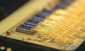
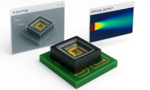
Inside the production

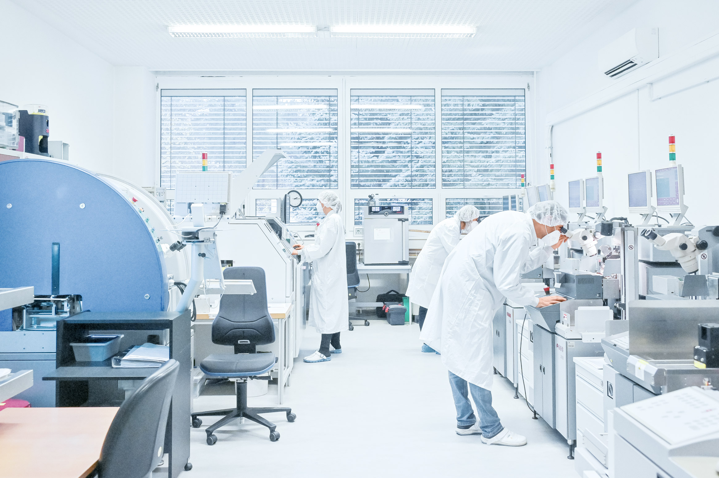
Industries
Processes & technical limits
| Processes | Tolerance | Max. part | Weight | Lot size | Materials |
|---|---|---|---|---|---|
| Chip Fabrication (Lithography, Metallization, Etching, Dicing, Mapping, Binning)Semiconductor manufacturing | – | – | – | – | Semiconductors (LED and photodiode chips, 225 nm–2300 nm) |
| Photonic Assembly (Pick and Place, Wire Bonding, Encapsulation, Chip on Board, SMD and TO Packaging)Assembly | – | – | – | – | LED chips, Photodiodes |
| Test & Qualification (Burn-in, Reliability, Environmental Tests)Testing | – | – | – | – | LEDs, Photodiodes |
| R&D: optical, mechanical and electrical design, prototyping, product developmentEngineering | – | – | – | – | – |
Additional services
Reference customers
Quality
Test and qualification services include burn-in, reliability and environmental testing as well as supply chain management for LEDs and photodiodes.
| Evidence | Berlin Köpenick |
|---|---|
| Burn-in | |
| Reliability tests | |
| Environmental tests |
History
- Mitte der
Start of development of LED chips and photodiode chips for niche markets
- 2026
Trade fair presence at Photonics West in San Francisco (Booth #4205-39)
- 2026
Launch of the joint VCSEL chip development project “VAST” with the Technical University of Berlin
- 2026
Trade fair presence at VISION 2026 in Stuttgart (Hall 10, Booth 10C16, German joint booth / SpectroNet)