Thermal Chuck systems for wafer testing and debonding solutions for Advanced Packaging since 1970

ERS electronic GmbH
Germering · Barbing · Dallas, TX (USA) · Zhubei (Taiwan) · Shanghai (China)New on Amplifa
About ERS electronic
ERS electronic GmbH, headquartered in Germering near Munich, develops and manufactures thermal management solutions for the semiconductor industry. Founded in 1970, the company produced the first thermal chuck for wafer testing and, with over 10,000 chucks sold since 1972, of which around 85 % are still in operation, is regarded as the pioneer of thermal wafer testing technology. The product portfolio includes thermal chuck systems (AirCool®, AC3, AirCool® PRIME) with temperatures from -65 °C to +550 °C as well as machines for Advanced Packaging: thermal and photothermal debonding systems (ADM, APDM650, MDM, MPDM, LumosON™), warpage adjustment (WAT330) and the 3D wafer profiler Wave 3000. More than 25 % of the workforce are developers; over 95 % of production takes place at the company's own plant near Munich, enabling same-day prototyping from its own CAD/CAM chain. Materials processed include silicon, SiC, GaN and GaAs wafers as well as molded wafers and panels up to 650×650 mm. Customers include wafer probing, FOWLP/FOPLP manufacturing, and automotive and safety electronics; worldwide, more than two billion ICs have been debonded on ERS systems.
- Site
- Germering
- Processes
- Thermal Debonding (FOWLP), Thermal Debonding (FOPLP Panel-Level), PhotoThermal Debonding, Warpage Adjustment (TriTemp Slide), Warpage Metrology (3D Wafer Profiling), Thermal Wafer Testing (Wafer Probing Thermal Chucks), Laser Marking (Wafer/Panel Frontside, 1064 nm Diode-pumped), Temporary Carrier Bonding and Debonding (Panel-Level, 310 x 310 mm)
- Materials
- Silicon, Silicon Carbide, Gallium Nitride, Gallium Arsenide, Molded wafer/panel, Molded Wafer/Panel, AirCool® air cooling, ACP air management
- Certificates
- ISO 9001:2015
- Founded
- 1970
- Industries
- Semiconductor industry (wafer test/wafer probing), Advanced Packaging (FOWLP/FOPLP), Semiconductor test and production, Automotive and safety electronics, Automotive/safety electronics (tested ICs)
- 01
Design/Engineering (in-house development department)
- 02
CAM manufacturing at own plant (>95 % of production in-house)
- 03
Quality assurance by an independent QA group
- 04
SECS/GEM integration and commissioning
- 05
Customer service/support and warpage adjustment
Materials & Processes
Silicon
Standard substrate material for wafer testing and thermal debonding up to 330 mm.
Silicon Carbide
Wide-bandgap semiconductor material processed on ERS debonding systems.
Gallium Nitride
Material for power semiconductors, compatible with ERS debonding and warpage processes.
Gallium Arsenide
III-V semiconductor material for RF applications in thermal debonding.
Molded Wafer/Panel
Reconstituted wafers and panels for FOWLP/FOPLP, panels up to 650×650 mm.
AirCool® air cooling
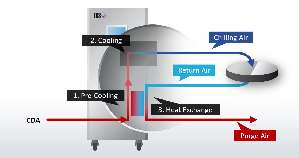
Patented cooling using CDA as the sole refrigerant, introduced in the early 1990s.
ACP air management
Patented two-pass heat exchanger system of the AC3 with turbo cooling and icing prevention.
TriTemp Slide
Contactless thermal conditioning and transport process for warpage correction of reconstituted wafers and panels.
Laser Marking (1064 nm)
Diode-pumped laser scribing for wafer/panel frontside marking and traceability.
Locations
Germering
DEHeadquarters (Stettiner Straße 3+5), production near Munich
- Materials
- Silicon, SiC, GaN, GaAs, molded wafer
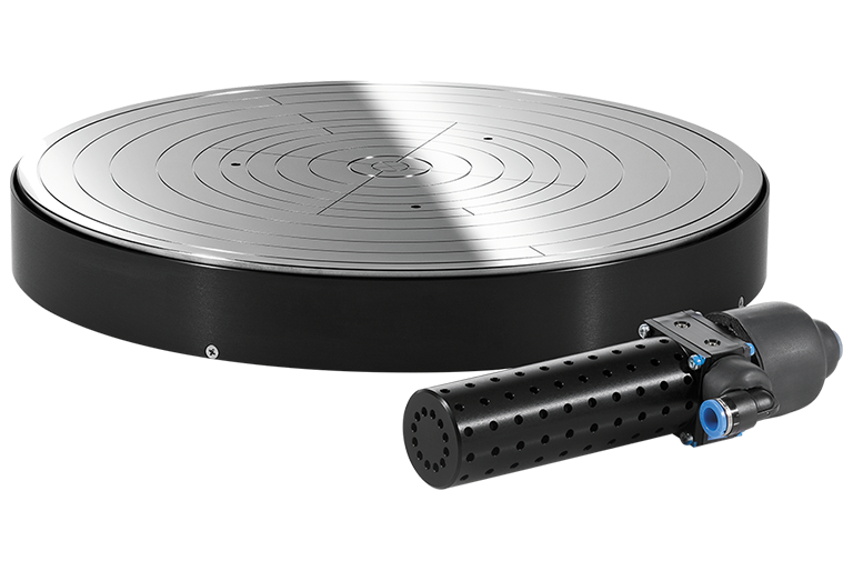
- Thermal chuck systems AirCool®, AC3, AirCool® PRIME
- ADM200/ADM330 Gen 3
- MDM200/MDM330
- CAD/CAM machine fleet
- Thermal imaging tools
Barbing
DEProduction and R&D site ERS Barbing, Competence Center Advanced Packaging (Liebigstraße 1)
- Materials
- Molded wafer/panel
- APDM650
- MPDM
- WAT330
- Wave 3000
- LumosON™ LUM300A/LUM600S1
Dallas, TX
USERS Americas – sales/support
Zhubei
TWERS Taiwan – sales/demonstration center
Shanghai
CNERS China – sales/support
Components & Systems
Inside the production
Industries
Processes & technical limits
| Processes | Tolerance | Max. part | Weight | Lot size | Materials |
|---|---|---|---|---|---|
| Thermal Debonding (FOWLP)Additive | – | 330 mm wafer | – | – | Silicon, Silicon Carbide (SiC), Gallium Nitride (GaN), Gallium Arsenide (GaAs), Molded wafer |
| Thermal Debonding (FOPLP Panel-Level)Additive | – | 650 x 650 mm × 650 mm | – | – | Molded panel, Silicon, Silicon Carbide (SiC), Gallium Nitride (GaN), Gallium Arsenide (GaAs) |
| PhotoThermal DebondingAdditive | – | – | – | – | Molded wafer/panel, Silicon, Silicon Carbide (SiC), Gallium Nitride (GaN), Gallium Arsenide (GaAs) |
| Warpage Adjustment (TriTemp Slide)Heat treatment | – | – | – | – | Silicon, Molded wafer/panel |
| Warpage Metrology (3D Wafer Profiling)Testing | – | – | – | – | – |
| Thermal Wafer Testing (Wafer Probing Thermal Chucks)Testing | – | 300 mm wafer (200 mm available) | – | – | – |
| Laser Marking (Wafer/Panel Frontside, 1064 nm Diode-pumped)Surface | – | – | – | – | – |
| Temporary Carrier Bonding and Debonding (Panel-Level, 310 x 310 mm)Additive | – | 310 x 310 mm × 310 mm | – | – | – |
13 Anlagen & Maschinen
| Machine | Manufacturer / model | Quantity | Working area | Year built | Site |
|---|---|---|---|---|---|
| Thermal Chuck System | ERS electronic AirCool® | – | – | – | Germering/Munich |
| Thermal Chuck System | ERS electronic AirCool® PRIME | – | 200 mm and 300 mm wafers | 2018 | – |
| Thermal Chuck System | ERS electronic AC3 (AC3 Fusion, ACP technology) | – | – | – | – |
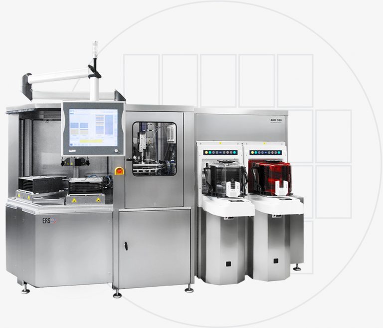
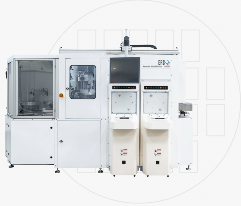
| Automatic Debond Machine | ERS electronic ADM330 (Gen 3) | – | 300/330 mm wafers; 3126 x 1856 x 2105 mm; temperature RT to +240°C; max. input warpage ±5 mm | – | Germering |
| Automatic Debond Machine | ERS electronic ADM200 | – | 200 mm wafers | – | – |
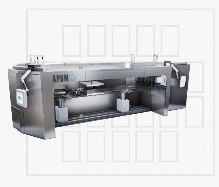
| Automatic Panel Debond Machine | ERS electronic APDM650 | – | Panels up to 650 x 650 mm; temperature RT-260°C; uniformity ±3°C; 4.6 x 3 m | 2021 | – |
| Manual/Semi-automatic Debond Machine | ERS electronic MDM200 / MDM330 | – | 200/300/330 mm wafers; temperature -10°C to +260°C; 2000 x 1050 x 1600 mm; 600 kg | – | – |
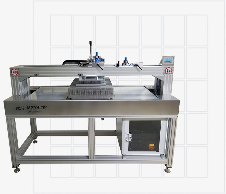
| Manual Panel Debond Machine | ERS electronic MPDM | – | Panels up to 615 x 615 mm, wafers 200/300 mm; temperature -10°C to 260°C; input warpage ±10 mm | – | – |
| Automatic Warpage Adjust Tool | ERS electronic WAT330 | – | – | 2023 | – |
| 3D Wafer Profiler | ERS electronic Wave 3000 | – | – | 2024 | – |
| PhotoThermal Debond Machine (Automatic) | ERS electronic LumosON™ LUM300A | – | – | – | – |
| PhotoThermal Debond Machine (Semi-Automatic, Wafer and Panel) | ERS electronic LumosON™ LUM600S1 | – | – | – | – |
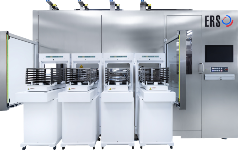
| Fully Automated Panel-Level Packaging System | ERS electronic | – | 310 x 310 mm substrates; 13 panels per hour | 2026 | – |
Additional services
Reference customers
Quality
An independent QA group with direct access to development and manufacturing monitors product quality throughout. ERS is certified to ISO 9001:2015 by TÜV SÜD (certificate 12 100 30597 TMS, valid until 2028-02-07).
| Evidence | Germering | Barbing |
|---|---|---|
| ISO 9001:2015 |
History
- 1970
ERS produces the first thermal chuck for wafer testing.
- 1972
Since 1972, over 10,000 chucks have been sold, approximately 85 % of which are still in operation today.
- Späte 1980er
True production cold testing in automatic wafer probers becomes possible for the first time with the ERS SuperCool®.
- Anfang der
Conversion to purely air-cooled systems; introduction of AirCool® technology with CDA as the sole refrigerant.
- 2005
Introduction of the AC3 system with patented ACP air management technology.
- 2009
Delivery of the first automatic 200-mm system (ADM200).
- 2011
Delivery of the first automatic 300-mm system (ADM330).
- 2018
Delivery of the first manual panel-level system (MPDM); introduction of AirCool® PRIME (300 mm, later 200 mm); partnership with Woowon Technology (Korea).
- 2019
Microworld (France) becomes sales partner for France, Switzerland and North Africa.
- 2021
Announcement of the automatic panel-level machine APDM650 (up to 650×650 mm).
- 2022
Market launch of ADM330 Gen 3, WAT330 and the Wave 3000 3D wafer profiler.
- 2024
Global Marketing Services (India) becomes sales partner; opening of the production and R&D site ERS Barbing including the Competence Center Advanced Packaging.
- 2025
New ISO 9001:2015 certification by TÜV SÜD (valid until 2028).
- 2026
Announcement of a fully automatic panel-level packaging system for 310×310-mm substrates.