Optical metrology and inspection systems as well as services for the semiconductor industry

EUMETRYS GmbH
New on Amplifa
About EUMETRYS
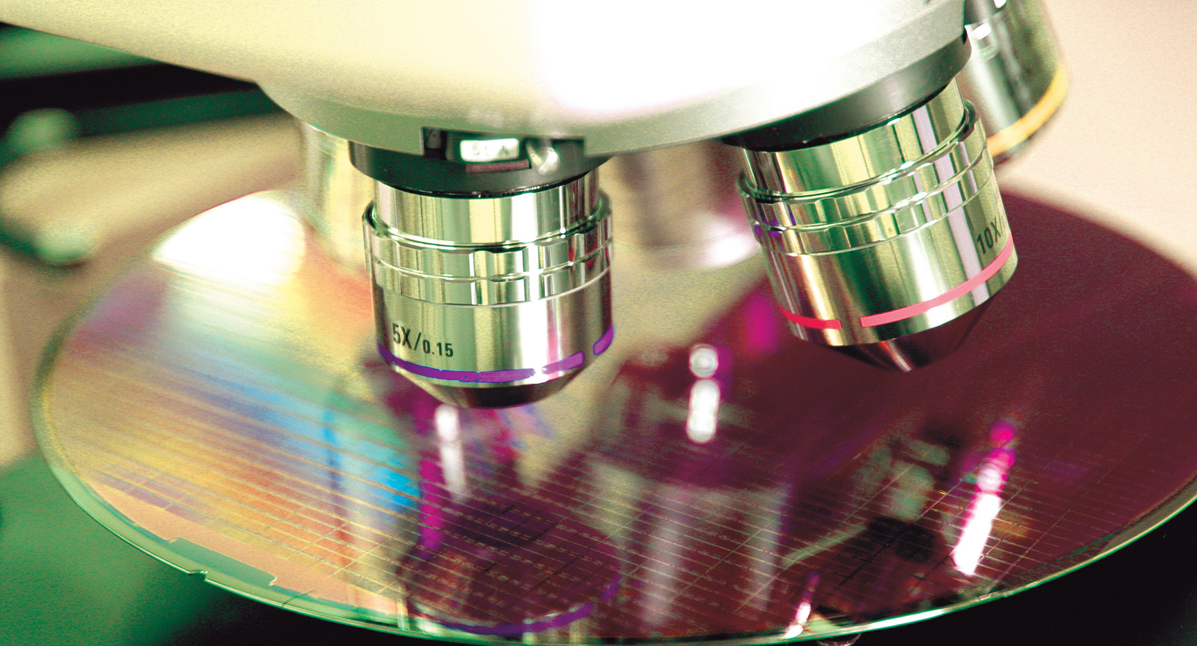
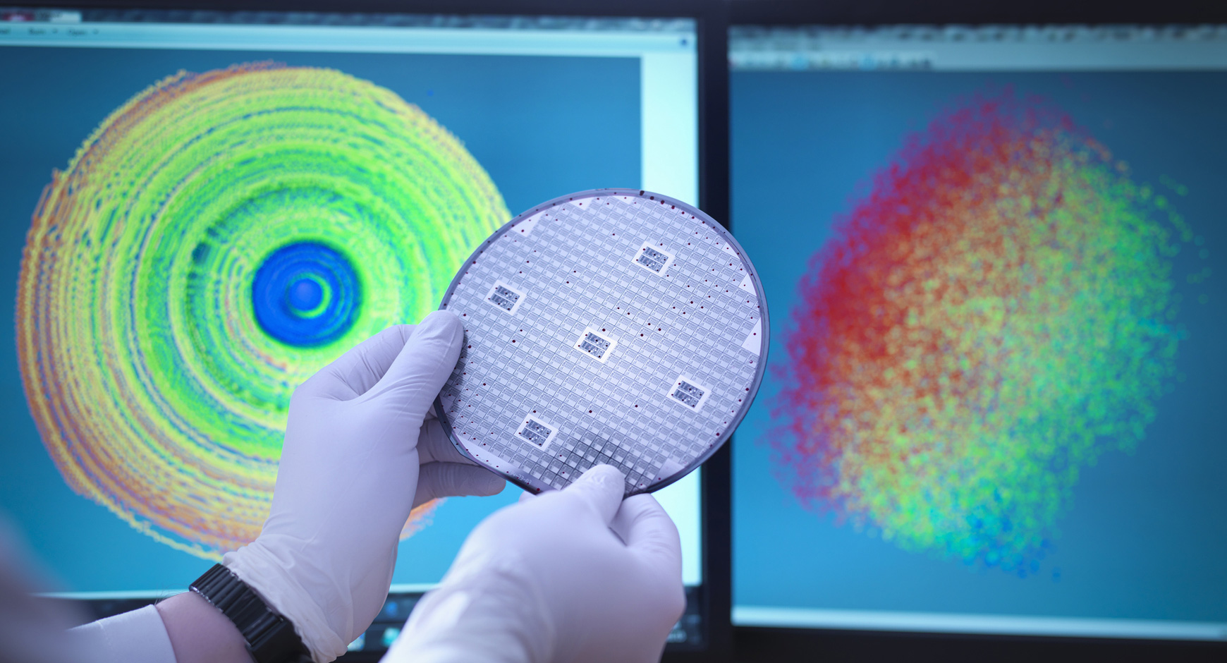
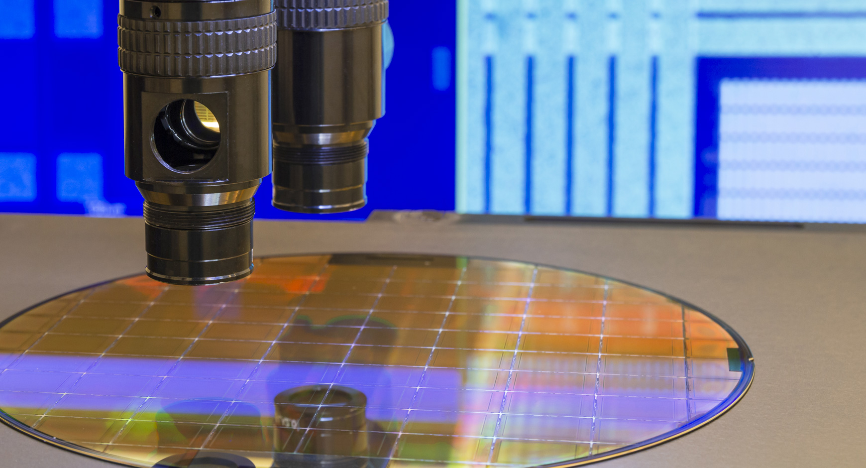
EUMETRYS is a company specializing in optical metrology and inspection for the semiconductor industry. The portfolio includes IVS systems for CD and overlay measurement, surface contamination analysis systems (YGK), photoluminescence mapping (ETAMAX PLATO), classification of crystal defects and stacking faults in SiC (MiPLATO SiC), Micro-LED review systems, and the all-in-one measurement system MICROSCAN for VIS and NIR applications. New and remanufactured systems are distributed to semiconductor manufacturers and laboratories. In addition, EUMETRYS offers preventive and corrective maintenance, multi-level training, process and data analysis, and robot services in Europe, Asia, and North America. Target industries are standard and compound semiconductors (III-V), MEMS, LED, substrates, telecommunications, VCSEL, and power devices. Since November 2022, a subsidiary, EUMETRYS GmbH, has been based in Germany.
- Processes
- Optical Metrology (IVS, CD and overlay measurement), Particles inspection / surface contamination analysis, Layer thickness measurement, Photoluminescence (PL) mapping / micro and macro PL for VIS and NIR, Crystal defect and stacking fault classification, Micro LED Review, Process analysis and qualification of steppers, Preventive and corrective maintenance, training
- Materials
- SiC (silicon carbide), III-V semiconductors, MEMS/LED substrates, Silicon semiconductor wafers, Inspectrology IVS (CD & Overlay), Surface contamination analysis, PL mapping (ETAMAX), Crystal defect classification
- Industries
- Semiconductor industry, Compound semiconductors (III-V), MEMS, LED / Micro-LED, Substrates, Telecommunications / Waveguides
- 01
Consulting and process analysis
- 02
Sales of new and remanufactured metrology systems
- 03
Commissioning and qualification
- 04
Preventive and corrective maintenance
- 05
Training and data analysis
Measurement Systems & Methods
Inspectrology IVS (CD & Overlay)
Optical metrology system for CD and overlay measurement on semiconductor wafers.
Surface contamination analysis
Particle inspection on opaque and transparent substrates.
PL mapping (ETAMAX)
Micro and macro photoluminescence mapping for VIS and NIR applications.
Crystal defect classification
Classification of crystal defects and stacking faults in SiC.
Micro LED Review
Review system for Micro-LED substrates.
All-in-one VIS/NIR measurement system
Combined measurement system for VIS and NIR applications.
Systems & Products


Inside the production

Industries
Processes & technical limits
| Processes | Tolerance | Max. part | Weight | Lot size | Materials |
|---|---|---|---|---|---|
| Optical Metrology (IVS, CD and overlay measurement)Inspection | – | – | – | – | Semiconductor wafers, III-V semiconductors, SiC |
| Particles inspection / surface contamination analysisInspection | – | – | – | – | Opaque and transparent substrates |
| Layer thickness measurementInspection | – | – | – | – | Semiconductor wafers |
| Photoluminescence (PL) mapping / micro and macro PL for VIS and NIRInspection | – | – | – | – | SiC, III-V semiconductors |
| Crystal defect and stacking fault classificationInspection | – | – | – | – | SiC |
| Micro LED ReviewInspection | – | – | – | – | Micro LED substrates |
| Process analysis and qualification of steppersEngineering | – | – | – | – | – |
| Preventive and corrective maintenance, trainingEngineering | – | – | – | – | – |
6 Anlagen & Maschinen
| Machine | Manufacturer / model | Quantity | Working area | Year built | Site |
|---|---|---|---|---|---|
| Optical metrology and inspection system (CD & overlay) | Eumetrys / Inspectrology IVS | – | – | – | – |
| Surface contamination analysis system | YGK | – | – | – | – |
| Photoluminescence mapping system | ETAMAX PLATO | – | – | – | – |
| Crystal defect / stacking fault classification system | ETAMAX MiPLATO SiC | – | – | – | – |
| Micro LED review system | Eumetrys / ETAMAX MICRO LED | – | – | – | – |
| All-in-one VIS/NIR measurement system | Eumetrys / ETAMAX MICROSCAN | – | – | – | – |
Additional services
History
- 2020
Presentation of the products via 3D virtual reality technology on the website (December 2020).
- 2022
CEO Yannick Bedin interviewed on BFM Business TV, program 'Décodage' (September 2022).
- 2022
Founding of the subsidiary EUMETRYS GmbH in Germany (November 2022).