Technical consulting, development and supply of components for OEM projects in optical measurement technology and cooling technology.
EURECA Messtechnik GmbH
CologneNew on Amplifa
About EURECA Messtechnik
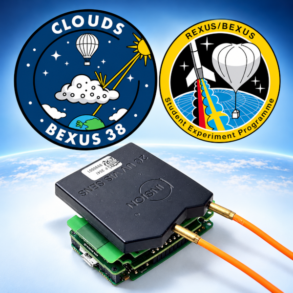
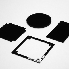
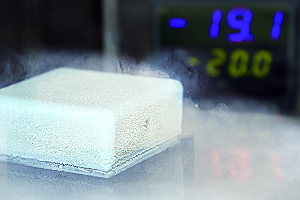
EURECA Messtechnik GmbH specializes in technical consulting, development and supply for OEM projects. Its focus areas are optical measurement technology systems, cameras and thermoelectric cooling systems. The company supports device manufacturers in developing new instruments and measurement methods and supplies the required components for series production – including CCD/CMOS image sensors, lenses, interference and IR filters made of plastic (PMMA), as well as Peltier elements and cooling system accessories. Its own services include the modification of image sensors, camera characterization, image simulations, the design of Peltier-based cooling systems, the assembly of Peltier elements and laser cutting of filter material with tolerances of ± 0.25 mm. In addition, EURECA offers seminars on optoelectronic components and operates as a distributor for machine vision cameras from Teledyne FLIR as well as a representative of Caeleste and CMOS Sensor Inc. The company is based in Cologne and participates in research projects such as quantumflexika and the CLOUDS experiment on board BEXUS-38.
- Site
- Köln
- Processes
- Laser cutting of filter material (PMMA), Laser cutting of various materials (sheet material 300 mm x 150 mm, up to 2000 mm x 3000 mm), Modification of CCD/CMOS image sensors (removal of cover glasses, attachment of special filters,, Assembly of Peltier elements (customized cable types and lengths,, Design and simulation of Peltier-based cooling systems, Development of customized Peltier elements and CCD/CMOS image sensors with driver electronics, Camera characterization (photo transfer curves), Simulation of CCD/CMOS images for assessing image quality without building prototypes
- Materials
- PMMA (plastic), Fused silica, Plastic (IR filter)
- Industries
- OEM device manufacturers, System integrators, Image processing/Machine Vision, Research/Quantum technologies, Research/Quantum technologies (education)
- 01
Technical consulting for OEM projects
- 02
Simulation (cooling systems, CCD/CMOS images)
- 03
Development of customized sensors and Peltier elements
- 04
Laser cutting of filter material
- 05
Assembly of Peltier elements
- 06
Supply of components for series production
Materials and Processes
PMMA (plastic)
Primary processed substrate for laser-cut filters, available in thicknesses from 0.5 to 3 mm.
Plastic (IR filter)
Material for cost-effective IR filters with an in-house cutting service.
Fused silica
Listed as a substrate material in the optics/filter range.
Locations
Cologne
DEHeadquarters with consulting, development, cutting service and assembly
- Materials
- PMMA, plastic
Products and Components
Inside the production
Industries
Processes & technical limits
| Processes | Tolerance | Max. part | Weight | Lot size | Materials |
|---|---|---|---|---|---|
| Laser cutting of filter material (PMMA)Other | ± 0,25 mm | 200 mm × 150 mm | – | – | PMMA, plastic |
| Laser cutting of various materials (sheet material 300 mm x 150 mm, up to 2000 mm x 3000 mm)Other | ± 0,25 mm | 3000 mm × 2000 mm | – | – | PMMA, plastic |
| Modification of CCD/CMOS image sensors (removal of cover glasses, attachment of special filters,Surface | – | – | – | – | glass, plastic |
| Assembly of Peltier elements (customized cable types and lengths,Assembly | – | – | – | – | plastic |
| Design and simulation of Peltier-based cooling systemsEngineering | – | – | – | – | – |
| Development of customized Peltier elements and CCD/CMOS image sensors with driver electronicsEngineering | – | – | – | – | – |
| Camera characterization (photo transfer curves)Testing | – | – | – | – | – |
| Simulation of CCD/CMOS images for assessing image quality without building prototypesEngineering | – | – | – | – | – |
| In-house cutting service for plastic-based IR filtersOther | – | – | – | – | plastic |
Additional services
History and Research
- 2018
Publication of the technical article »Image Simulation and Analysis« by Karsten Sengebusch in the journal »Optik & Photonik« (12.06.2018).
- 2026
CLOUDS experiment with EURECA dual micro-spectrometer on board BEXUS-38 (stratospheric flight, Esrange, Sweden).
- 2026
Participation in the research project quantumflexika (10/2026–09/2029) with Osnabrück University and Paderborn University, funded by the Federal Ministry for Research, Technology and Space.