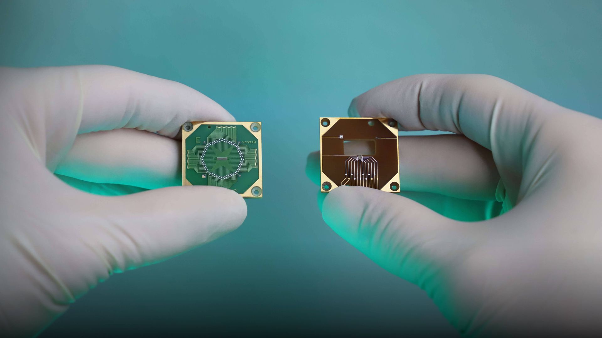
Probe cards with micro-3D-printed metal probes and CERES µAM printing systems for the semiconductor industry

Exaddon AG
Glattbrugg (CH)New on Amplifa
About Exaddon
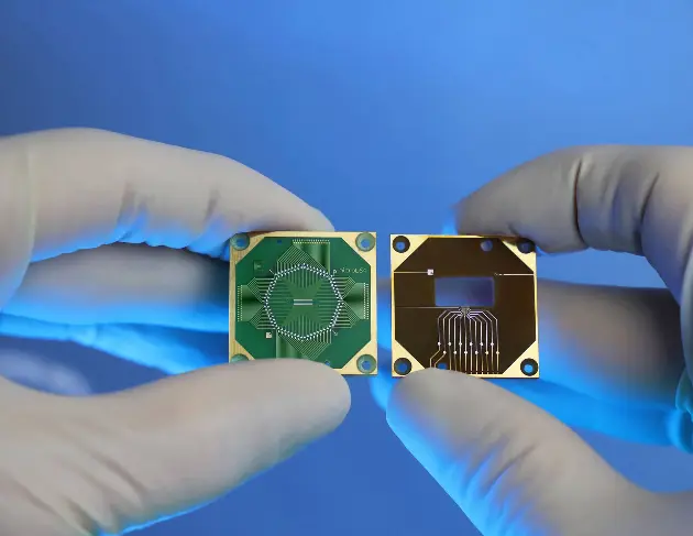
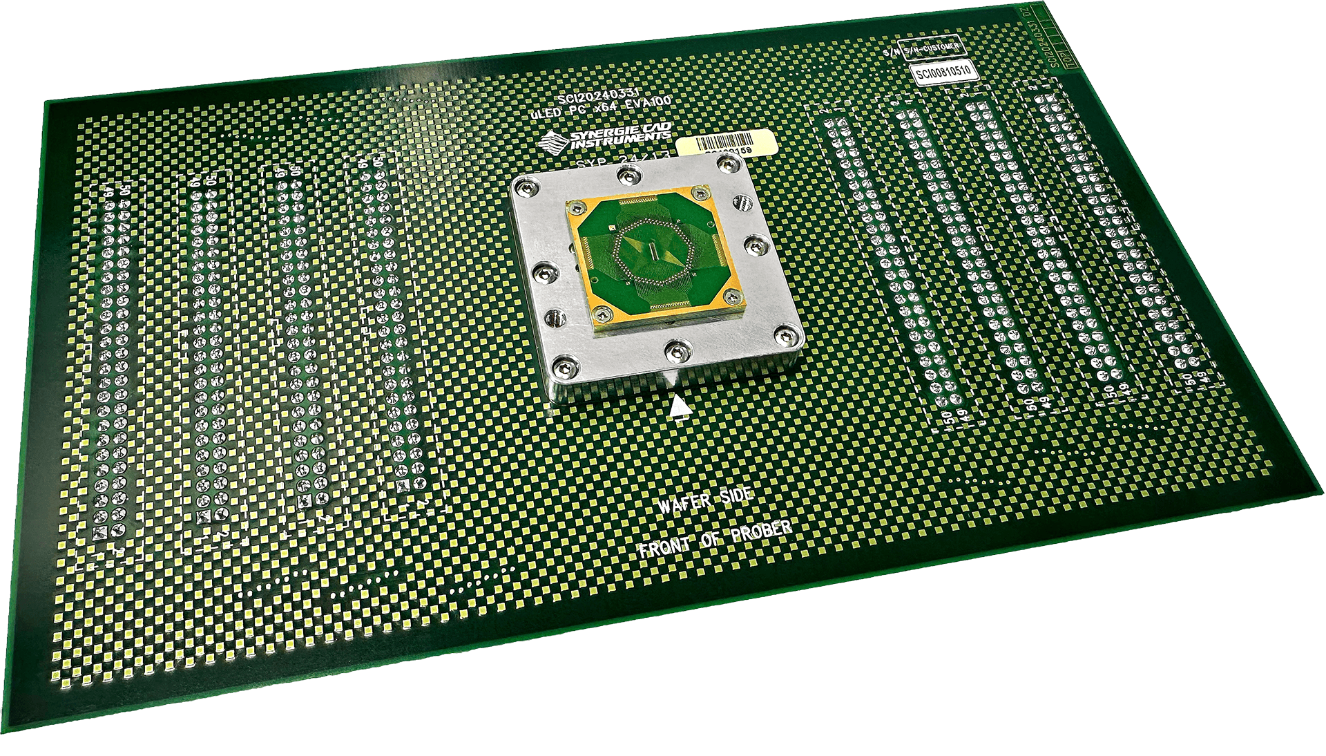
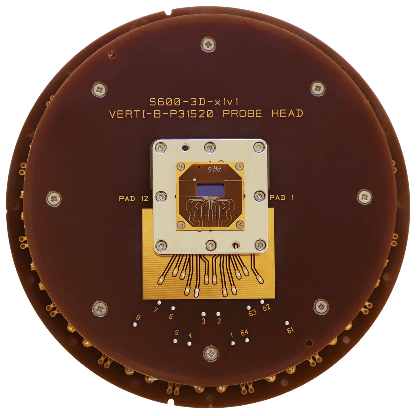
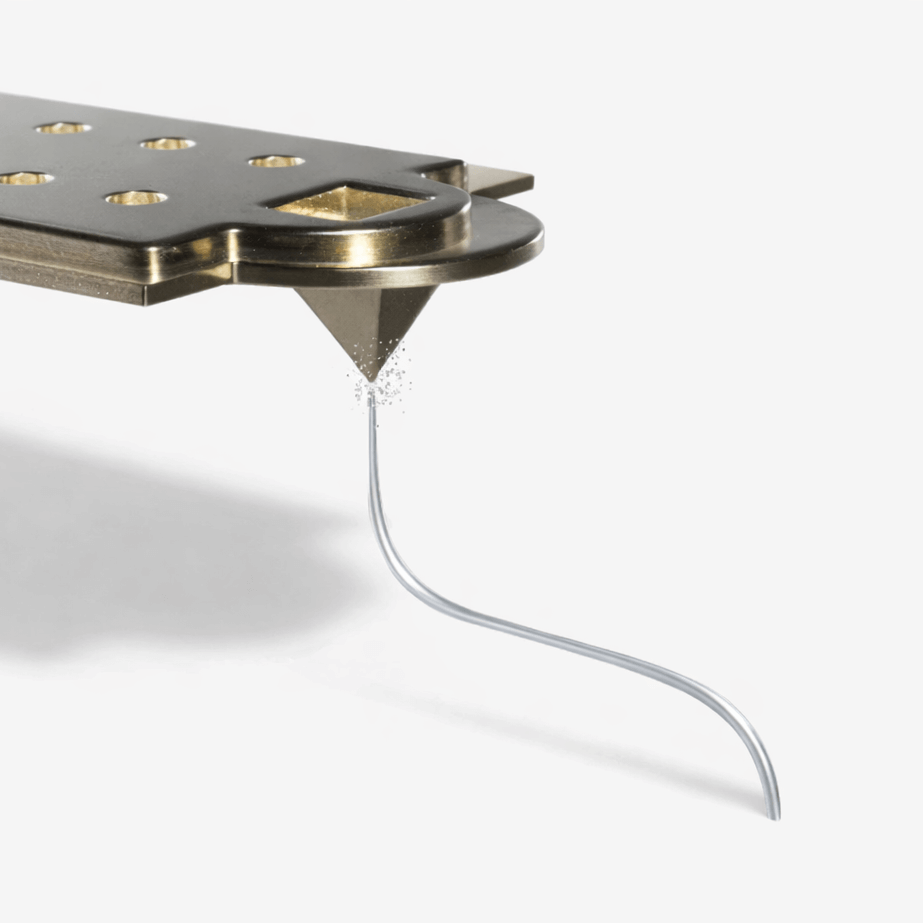
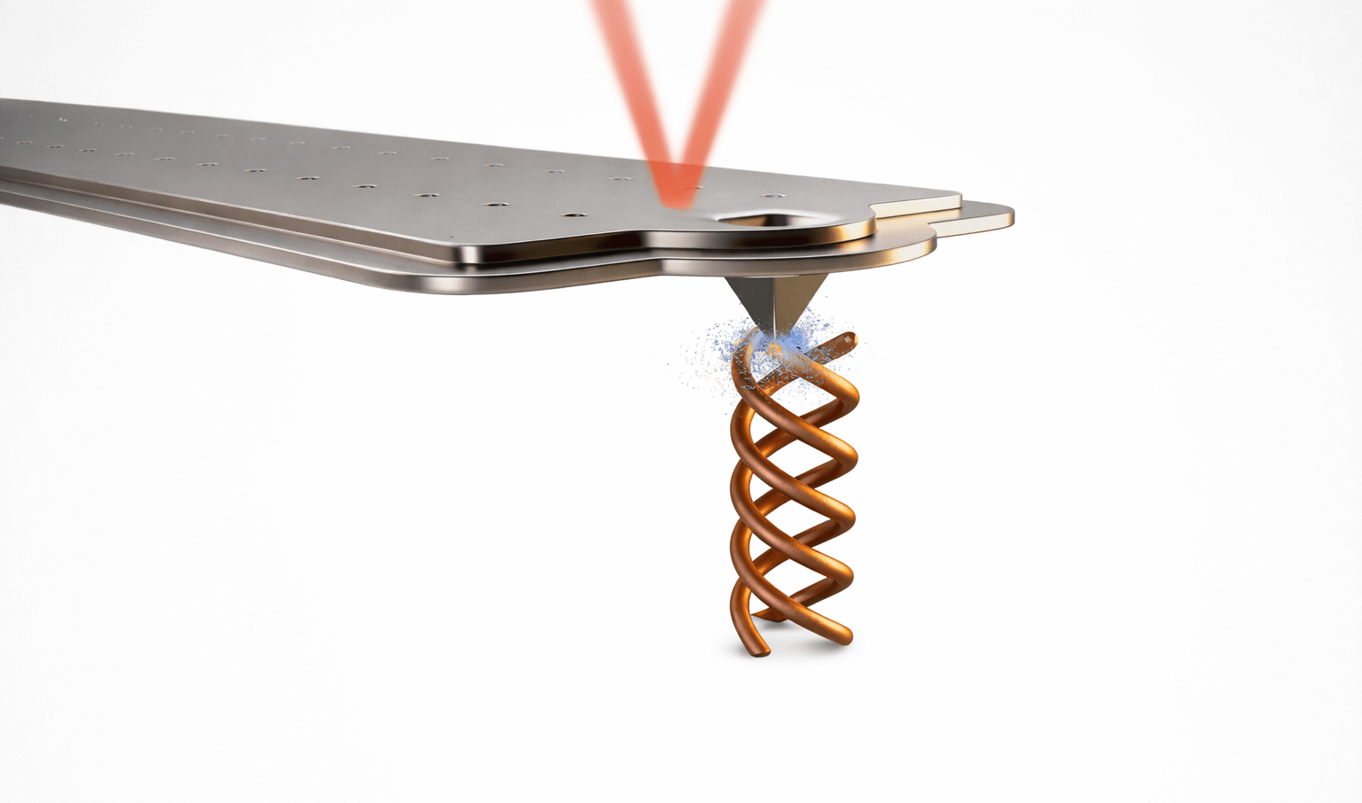
Exaddon AG is a Swiss company based in Glattbrugg (Canton Zurich) that emerged from the business unit of Cytosurge and has operated as an independent AG since 2019. The company manufactures probe cards with micro-3D-printed metal probes for advanced wafer testing in the semiconductor industry, in particular for MicroLED electroluminescence testing and Parametric/Wafer Acceptance Testing. The foundation is a proprietary metal micro-3D printing technology (µAM) based on localized electrodeposition with an Iontip nozzle of 300 nm aperture, which allows freeform geometries with sub-micrometer precision. Materials are microcrystalline copper (density > 99 %, approximately 87 % of the conductivity of bulk copper), gold, and nickel as a coating shell. In addition to probe cards, Exaddon sells the CERES µAM printing system including installation and training, and develops customer-specific probes from feasibility assessment to prototype. Customers include semiconductor and display manufacturers, high-frequency technology (mmWave/5G/THz), and research institutes such as Georgia Tech, KIT, EMPA, and MPIE.
- Site
- Glattbrugg
- Processes
- Wafer-level testing with probe cards (micro-3D printed probes), MicroLED electroluminescence (EL) testing (probe card), Parametric / Wafer Acceptance Testing (WAT) probe card, Application-specific custom probes (development from feasibility to prototype), Metal micro-3D printing (µAM / localized electrodeposition, LECD-µAM), Manufacturing of high-frequency components (mmWave/5G/THz waveguides, helices, interconnects), Micro-3D printing (µAM) of metal microstructures, Probe cards for wafer testing (MicroLED EL testing, Parametric/WAT, custom probes)
- Materials
- Copper (micro-3D printed, microcrystalline), Gold, Nickel (coating shells), Copper (micro-3D-printed, microcrystalline), Nickel (coating), Metal micro-3D printing (localized electrodeposition)
- Founded
- 2019
- Industries
- Semiconductor industry, Wafer testing, MicroLED display technology, High-frequency technology (mmWave/5G/THz), Telecommunications, Research
- 01
Application and requirement review
- 02
Feasibility assessment and concept design
- 03
Micro-3D printing of probe structures (CERES µAM)
- 04
Prototype manufacturing and evaluation
- 05
Integration into probe card and delivery
Materials & Processes
Copper (micro-3D-printed, microcrystalline)
Conductive probe and microstructures with > 99 % density and approximately 87 % of the conductivity of bulk copper.
Gold
Printed structures for applications with the highest conductivity and contact requirements.
Nickel (coating)
250 nm thin nickel shells increase the strength of copper microstructures by approximately a factor of three.
Metal micro-3D printing (localized electrodeposition)
Freeform shaping of micro- to sub-mm structures with sub-micrometer resolution without masks.
Sites
Glattbrugg
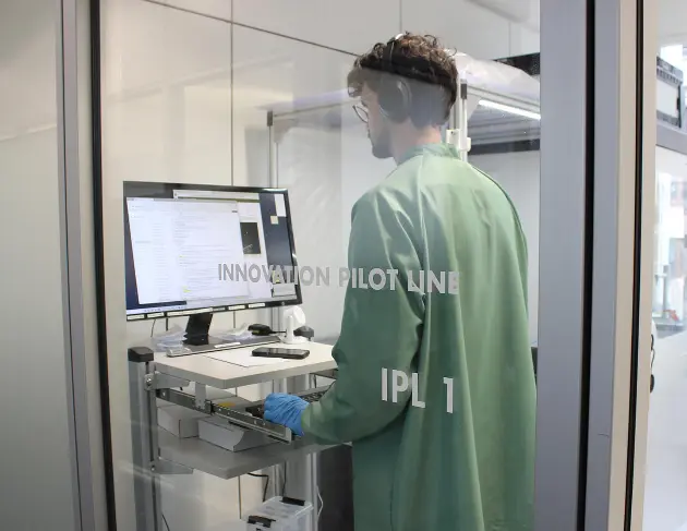
CHHeadquarters with manufacturing (Innovation Pilot Line) and CERES system sales
- Part weight / size
- Micro- to sub-mm structures
- Lot size
- Prototype to small series
- Materials
- Copper, gold, nickel
- CERES µAM metal micro-3D printing system
- Innovation Pilot Line (3D printing of wafer probing arrays)
Components
Inside the production
Industries
Processes & technical limits
| Processes | Tolerance | Max. part | Weight | Lot size | Materials |
|---|---|---|---|---|---|
| Wafer-level testing with probe cards (micro-3D printed probes)Testing | – | – | – | – | Copper, Gold |
| MicroLED electroluminescence (EL) testing (probe card)Testing | Ultrafine pitch < 20 µm | – | – | – | Copper |
| Parametric / Wafer Acceptance Testing (WAT) probe cardTesting | Ultrafine pitch < 20 µm; ultra-low background leakage < 1 | – | – | – | Copper |
| Application-specific custom probes (development from feasibility to prototype)Engineering | – | – | – | – | – |
| Metal micro-3D printing (µAM / localized electrodeposition, LECD-µAM)Additive | Sub-micrometer precision; nozzle aperture 300 nm | Sub-mm | – | – | Copper, Gold, Nickel (coating) |
| Manufacturing of high-frequency components (mmWave/5G/THz waveguides, helices, interconnects)Additive | Sub-micrometer precision; 66 GHz, >155 GHz operation | – | – | – | Copper, Gold |
2 Anlagen & Maschinen
| Machine | Manufacturer / model | Quantity | Working area | Year built | Site |
|---|---|---|---|---|---|
| CERES µAM metal micro-3D printing system (localized electrodeposition, Iontip nozzle with 300 nm | Exaddon CERES | – | Micro- to sub-mm structures, sub-micrometer resolution | – | Exaddon AG, Glattbrugg (Switzerland) |
| Innovation Pilot Line (3D printing of wafer probing arrays) | Exaddon | – | – | – | Exaddon AG, Glattbrugg (Switzerland) |
Additional services
Reference customers
History
- 2019
Spin-off of Exaddon as an independent company from the business unit of Cytosurge
- 2022
Partnership with Synergie Cad Instruments for ultra-low leakage parametric probe cards
- 2022
Best Paper Award of the journal Micromachines; research publications with EMPA, MPIE, Goethe University, and Jilin University/CUST
- 2025
Georgia Tech publishes D-band/sub-THz interconnect research with the CERES system (IEEE paper)
- 2026
KIT acquires a CERES µAM printing system for THz research; participation in SWTest in Carlsbad, USA