Machines for automated assembly and electro-optical testing of photonic devices – From Lab to Fab
ficonTEC Service GmbH
Achim (Rehland 8) · Achim (Im Finigen 3)New on Amplifa
About ficonTEC
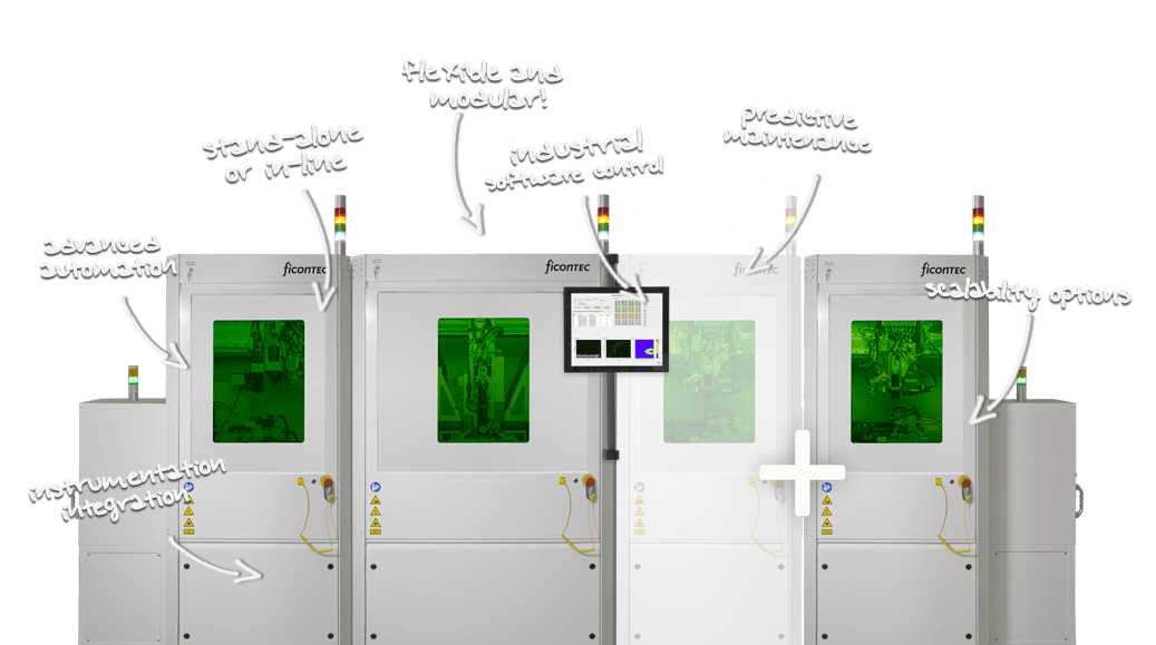
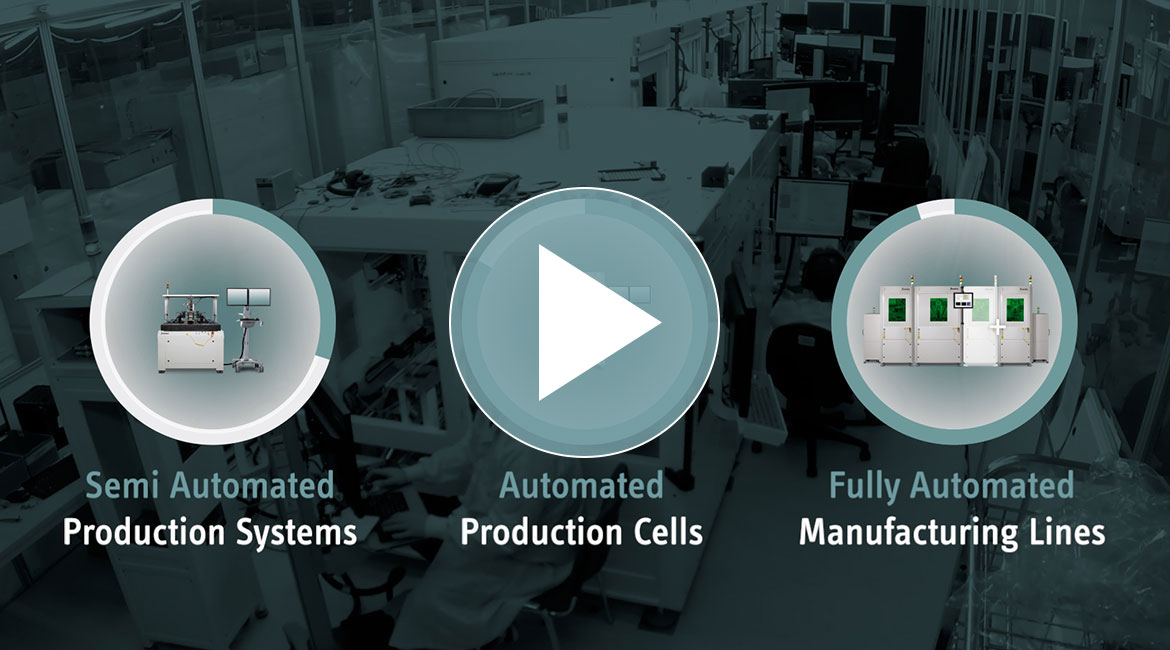
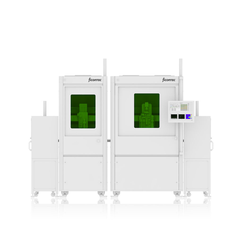
ficonTEC is a system provider for microsystem technology and develops, manufactures and services production machines for the photonic device industry. The portfolio includes automated die-level assembly (ASSEMBLYLINE), flexible align-&-attach platforms for R&D and low-volume production (CUSTOMLINE), electro-optical test equipment at die and wafer level (TESTLINE, WAFER TESTLINE), precision stacking of laser diode bars (STACKLINE) and Nd:YAG laser microwelding stations (LASER WELD), controlled by proprietary process software. The systems operate with sub-micron precision during passive and active multi-axis alignment of chips, fibers and PICs of various material systems. More than 2500 systems are installed worldwide (Q4 2026) in telecommunications, data communications, 5G infrastructure, 3D sensing, automotive/lidar, high-power diode lasers and silicon photonics for AI/CPO applications. From entry-level to inline high-volume systems, the modular architecture is scalable. The company's location and headquarters is Achim near Bremen.
- Site
- Achim
- Processes
- Photonics automated assembly (align-&-attach) – ASSEMBLYLINE, Photonics device assembly – CUSTOMLINE (align-&-attach, R&D/low-volume), Die-level photonic device test (mixed-signal electro-optical test) – TESTLINE, Wafer-level photonic device test (electro-optical probing) – WAFER TESTLINE, Precision stacking/unstacking of semiconductor laser diode bars – STACKLINE, Laser microwelding (2/3-beam Nd:YAG, multi-point/seam welding, post-weld shift correction) – LASER, Bonding using (UV-) epoxy compounds, Thermal-based or laser soldering
- Materials
- Photonics Integrated Circuits (PICs) – various material systems, Laser diode chips / VCSELs, Fibers (optical fiber components), UV-Epoxy / Epoxy compounds, Photonics Integrated Circuits (various material systems), Optical fibers / fiber components, UV epoxy / epoxy compounds, Nd:YAG laser microwelding (2- or 3-beam)
- Certificates
- ISO 9001:2015, ISO/IEC 27001:2022
- Industries
- Telecommunications, Data communications, 5G infrastructure, 3D sensing / smartphone, Automotive (lidar), Aerospace
- 01
Systems engineering
- 02
Process and software development
- 03
Machine manufacturing (microsystem technology)
- 04
Assembly & commissioning
- 05
Service & support
Materials & Processes
Photonics Integrated Circuits (various material systems)
Processed on all assembly and test platforms regardless of the PIC material system.
Laser diode chips / VCSELs
Target components for assembly, stacking and high-power diode laser manufacturing.
Optical fibers / fiber components
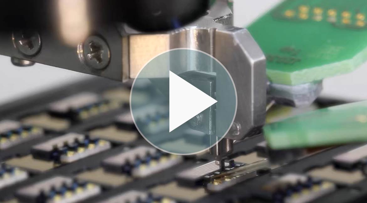
Positioning and fixing with sub-micron accuracy during align-&-attach.
UV epoxy / epoxy compounds
Bonding of optical components in assembly processes.
Nd:YAG laser microwelding (2- or 3-beam)
Multi-point or seam welding of ferruled optical components with post-weld shift correction.
Sites
Achim (Rehland 8)
DEHeadquarters, systems engineering, manufacturing and service; site as per ISO 9001 certificate
- Lot size
- Prototype to high volume (inline)
- Materials
- Photonic chips, PICs, fibers
- ASSEMBLYLINE
- CUSTOMLINE
- TESTLINE
- WAFER TESTLINE
- STACKLINE
- LASER WELD
- Process software
Achim (Im Finigen 3)
DEProcess and software development (as per ISO 27001 certificate)
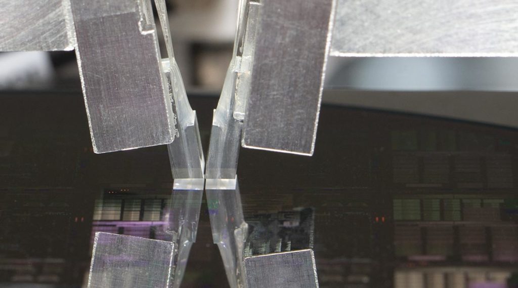
Inside the production
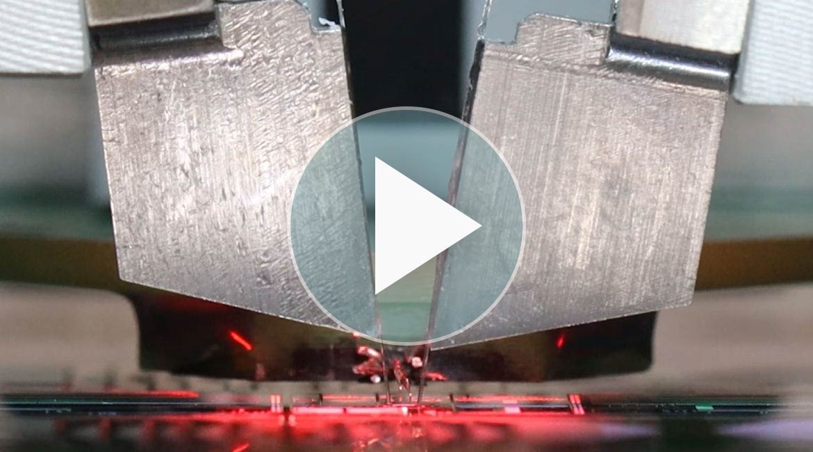
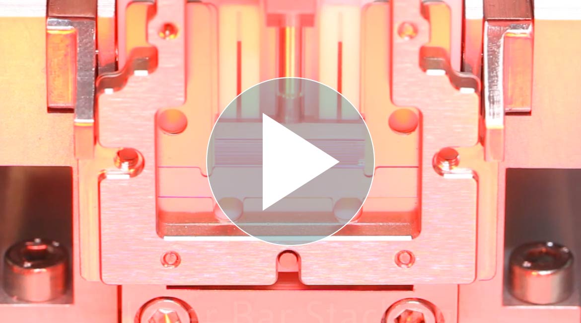
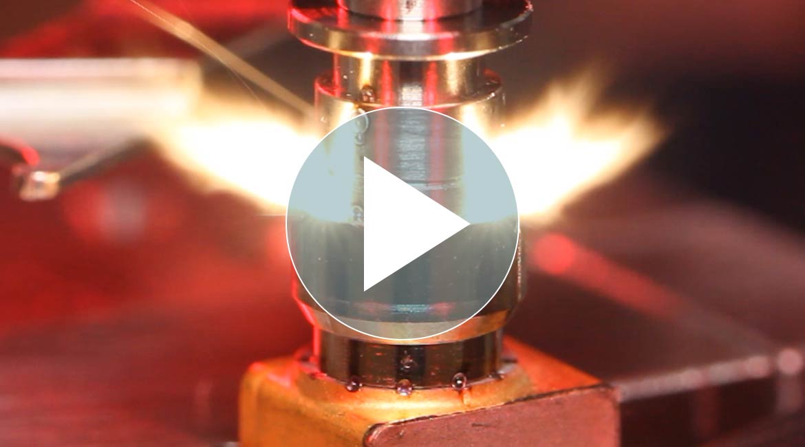
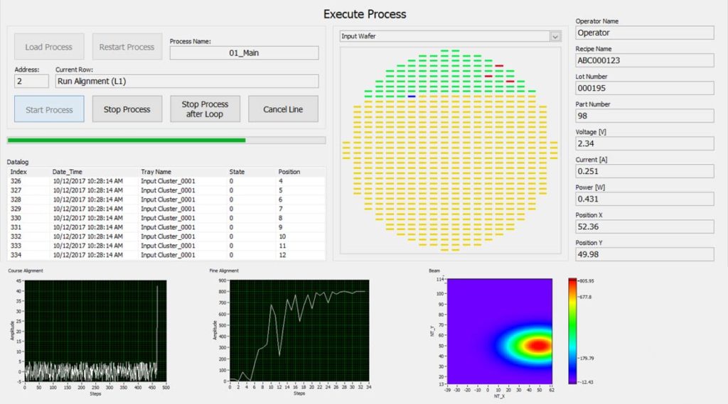
Industries
Processes & technical limits
| Processes | Tolerance | Max. part | Weight | Lot size | Materials |
|---|---|---|---|---|---|
| Photonics automated assembly (align-&-attach) – ASSEMBLYLINEAssembly | – | – | – | – | – |
| Photonics device assembly – CUSTOMLINE (align-&-attach, R&D/low-volume)Assembly | – | – | – | Low-Volume | – |
| Die-level photonic device test (mixed-signal electro-optical test) – TESTLINETesting | – | – | – | – | – |
| Wafer-level photonic device test (electro-optical probing) – WAFER TESTLINETesting | – | – | – | – | – |
| Precision stacking/unstacking of semiconductor laser diode bars – STACKLINEAssembly | +/- 2 µm (optional +/- 0,5 µm) | – | – | – | Semiconductor laser diode bars |
| Laser microwelding (2/3-beam Nd:YAG, multi-point/seam welding, post-weld shift correction) – LASERJoining | – | – | – | – | Ferruled optical components |
| Bonding using (UV-) epoxy compoundsJoining | – | – | – | – | UV-Epoxy, Epoxy compounds |
| Thermal-based or laser solderingJoining | – | – | – | – | – |
| Passive/active multi-axis sub-micron-accuracy component alignmentAssembly | Sub-micron | – | – | – | – |
| Burn-in testingTesting | – | – | – | – | – |
| LIV testsTesting | – | – | – | – | – |
| Beam and spectral characterizationTesting | – | – | – | – | – |
| Optical facet and side wall inspection (optional)Testing | – | – | – | – | – |
6 Anlagen & Maschinen
| Machine | Manufacturer / model | Quantity | Working area | Year built | Site |
|---|---|---|---|---|---|
| Automated photonic device assembly system | ficonTEC ASSEMBLYLINE | – | – | – | – |
| Flexible align-&-attach assembly platform | ficonTEC CUSTOMLINE | – | – | – | – |
| Die-level electro-optical test system | ficonTEC TESTLINE | – | – | – | – |
| Wafer-level electro-optical probing/test system | ficonTEC WAFER TESTLINE | – | – | – | – |
| Precision device stacking/unstacking system | ficonTEC STACKLINE | – | – | – | – |
| Nd:YAG laser microwelding station (2 or 3-beam) | ficonTEC LASER WELD | – | – | – | – |
Additional services
Quality & Certifications
ficonTEC is certified according to ISO 9001:2015 (DNV, systems engineering, manufacturing and service of microsystem technology machines) and ISO/IEC 27001:2022 (DQS, process and software development).
| Evidence | Achim (Rehland 8) | Achim (Im Finigen 3) |
|---|---|---|
| ISO 9001:2015 | ||
| ISO/IEC 27001:2022 |
History
- 2014
First ISO 9001 certification (by a different certification body, according to the DNV certificate)
- 2026
Over 2500 installed systems worldwide (Q4 2026); RoboTechnik Hong Kong listing; strategic cooperation with HTSI (Taiwan) for CPO test solutions