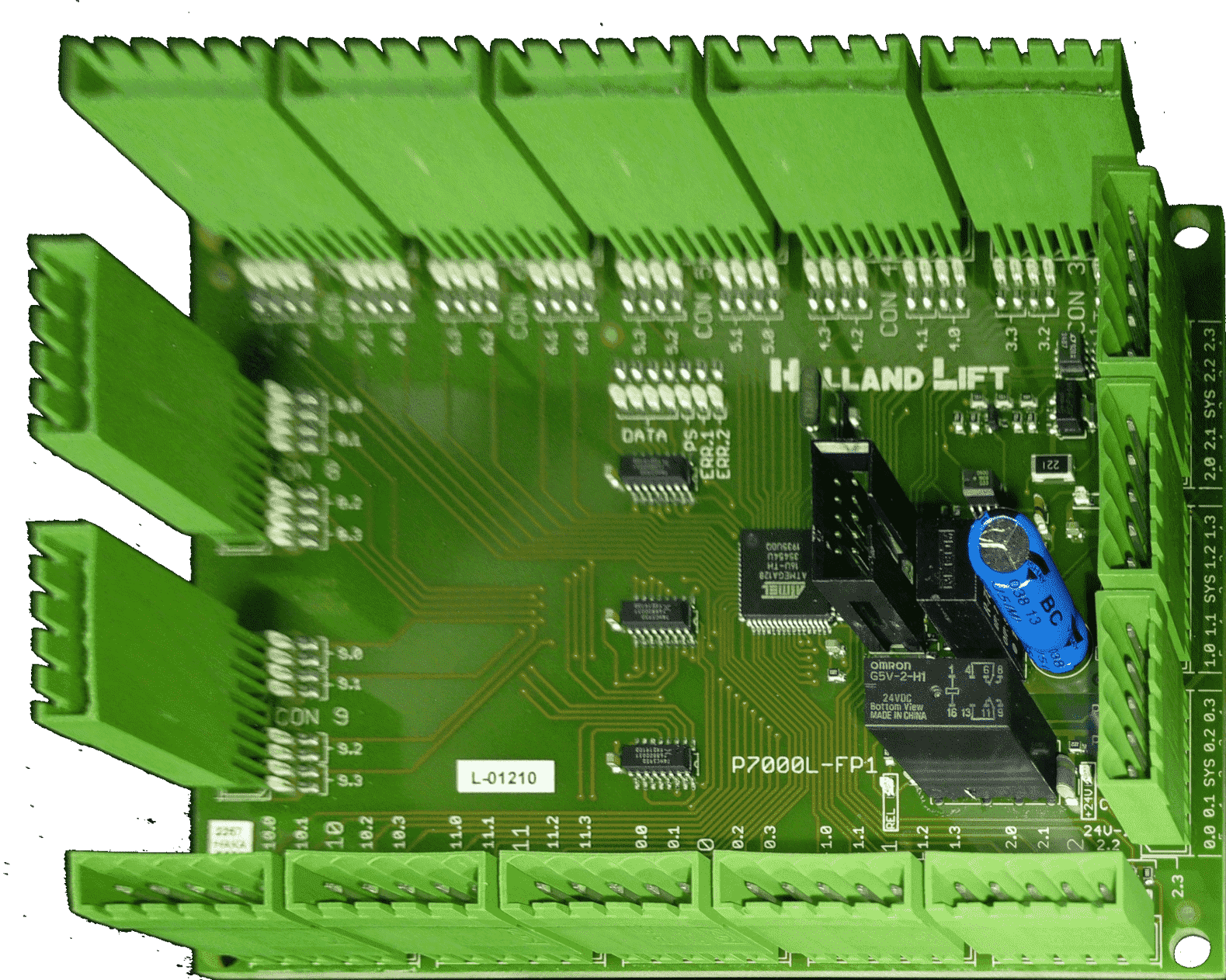
Manufacture of printed circuit boards and electronic assemblies including development, testing and material management.

HAKA Elektronik-Leiterplatten GmbH
Spiesen-ElversbergNew on Amplifa
About HAKA Elektronik-Leiterplatten
HAKA Elektronik-Leiterplatten GmbH has been active in the field of printed circuit board manufacturing and electronics development for over 30 years. The company manufactures single-sided and double-sided printed circuit boards as well as multilayers with options such as legend printing, deviating solder mask colors, scoring, chemically nickel/gold (Chem NiAu) surface finish and E-test. Following the commissioning of assembly production, the portfolio was expanded: SMD and THT placement, reflow soldering in a 3-chamber convection oven, selective soldering, rework, optical inspection, microscope checks and functional testing of assemblies and devices are all part of the service spectrum. In addition, HAKA offers electronics development, material management via smart ERP including the processing of customer material, as well as online tools such as a calculator, placement data visualization (PCB view) and utilities. The site is located in Spiesen-Elversberg in the Saarland; production is ESD-compliant and Made in Germany.
- Site
- Spiesen-Elversberg
- Processes
- Single-sided PCB manufacturing, Double-sided PCB manufacturing, Multilayer PCB manufacturing, Slot milling, Milled contour / contour milling, Nibbling (cut-outs from 0.5mm), Scoring of printed circuit boards, Drilling (metallized and non-metallized holes, min. 0.5mm non-metallized)
- Materials
- Copper (copper cladding, traces), Nickel (electroless Ni/Au surface finish, approx. 5µm), Gold (electroless Ni/Au surface finish, approx. 0.1µm), Tin (HAL surface finish, coating thickness covering up to 35µ; electroless Sn not offered), Solder mask, Base material (PCB base material, various thicknesses), Copper, Electroless Nickel/Gold (chem. NiAu)
- Certificates
- E-test (flying probe), Optical inspection, Functional testing, ESD-compliant production
- Industries
- Electronics, PCB/assembly manufacturing
- 01
Electronics development
- 02
PCB manufacturing (drilling, milled contour, slot milling, scoring, surface
- 03
E-test (flying probe)
- 04
Assembly manufacturing (SMD/THT placement, reflow and selective soldering)
- 05
Optical inspection and microscope checks
- 06
Rework and functional testing
- 07
Material management / smart ERP
Materials and Surfaces
Copper
Copper cladding and traces; other copper claddings available as an option.
Electroless Nickel/Gold (chem. NiAu)
Surface finish with approx. 5 µm nickel and approx. 0.1 µm gold; high flatness and long shelf life, unproblematic for fine-pitch structures.
HAL (hot air leveling, tin)
Tin surface finish covering up to 35 µm; very long shelf life and trouble-free multiple soldering.
Solder mask
Standard as well as different-colored solder mask available as an option; marking preferably in the solder mask of the solder side.
PCB base material
Various material thicknesses available; scoring requires a material thickness of at least 1.0 mm.
Site
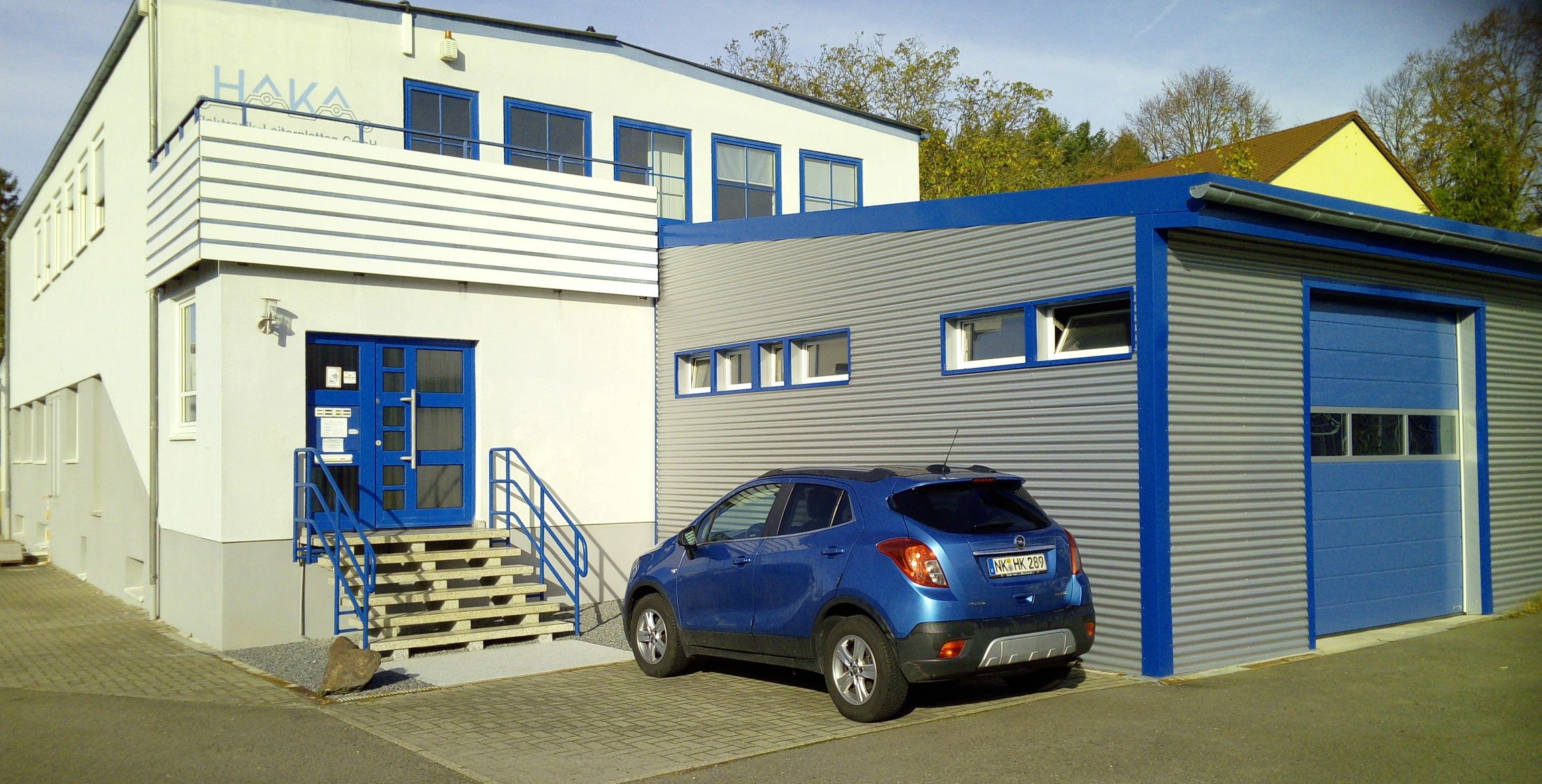
Spiesen-Elversberg
DEHeadquarters and production
- Lot size
- Prototypes, samples and series
- Materials
- PCB base material, copper, Ni/Au, HAL, solder mask
- Flying probe tester (E-test)
- 3-chamber reflow oven (convection oven)
- Selective soldering system
- Milling machine (contour/slot milling)
- Scoring machine
Components
Inside the production


Industries
Processes & technical limits
| Processes | Tolerance | Max. part | Weight | Lot size | Materials |
|---|---|---|---|---|---|
| Single-sided PCB manufacturingElectronics | – | – | – | – | Base material (printed circuit board) |
| Double-sided PCB manufacturingElectronics | – | – | – | – | Base material (printed circuit board) |
| Multilayer PCB manufacturingElectronics | – | – | – | – | Base material (printed circuit board) |
| Slot millingElectronics | – | Slot length max. 10mm | – | – | – |
| Milled contour / contour millingElectronics | +/- 0.2mm (2mm tool) | – | – | – | – |
| Nibbling (cut-outs from 0.5mm)Electronics | – | – | – | – | – |
| Scoring of printed circuit boardsElectronics | – | – | – | – | Base material with min. 1.0 mm material thickness |
| Drilling (metallized and non-metallized holes, min. 0.5mm non-metallized)Electronics | – | – | – | – | – |
| Marking (stamp)Surface | – | – | – | – | – |
| Legend printing on one or both sidesSurface | – | – | – | – | – |
| Chem NiAu (electroless nickel/gold surface finish)Surface | – | – | – | – | – |
| HAL (hot air leveling)Surface | – | – | – | – | – |
| E-test (electrical test, flying probe)Testing | – | – | – | – | – |
| Electronics developmentEngineering | – | – | – | – | – |
| SMD placementAssembly | – | – | – | – | – |
| THT placementAssembly | – | – | – | – | – |
| Reflow soldering (hot air soldering in a convection oven)Joining | – | – | – | – | – |
| Selective solderingJoining | – | – | – | – | – |
| Via filling with over-platingElectronics | – | – | – | – | – |
| Optical inspection and microscope checksTesting | – | – | – | – | – |
| Rework of printed circuit boards and assembliesAssembly | – | – | – | – | – |
| Functional testing of assemblies and devicesTesting | – | – | – | – | – |
| Material management / smart ERP / customer material processingEngineering | – | – | – | – | – |
5 Anlagen & Maschinen
| Machine | Manufacturer / model | Quantity | Working area | Year built | Site |
|---|---|---|---|---|---|
| Flying probe tester (E-test) | – | – | – | – | Spiesen-Elversberg |
| 3-chamber reflow oven (convection oven) | – | – | – | – | Spiesen-Elversberg |
| Selective soldering system | – | – | – | – | Spiesen-Elversberg |
| Milling machine (PCB contour/slot milling) | – | – | – | – | Spiesen-Elversberg |
| Scoring machine | – | – | – | – | Spiesen-Elversberg |
Additional services
Quality
The correct function of the printed circuit boards is verified fully automatically by electrical testing on flying probe testers (open circuits and short circuits). In addition, optical inspection, microscope checks and functional testing of assemblies and devices are performed; production is ESD-compliant.
| Evidence | Spiesen-Elversberg |
|---|---|
| E-test (flying probe) | |
| Optical inspection | |
| Functional testing | |
| ESD-compliant production |
History
Active in the field of printed circuit board manufacturing and electronics development for over 30 years.
Commissioning of assembly manufacturing and corresponding portfolio expansion.