Service provider for professional PCB layout: from schematic entry to manufacturing data and prototype procurement.

HD-Design GmbH
61194 NiddatalNew on Amplifa
About HD-Design
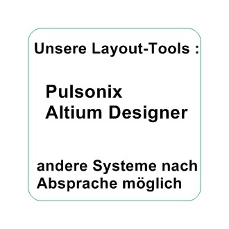
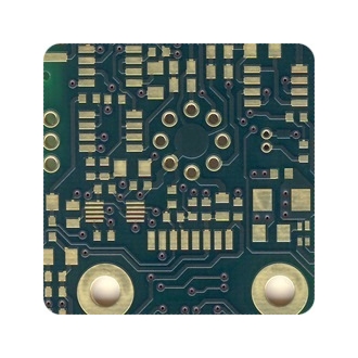
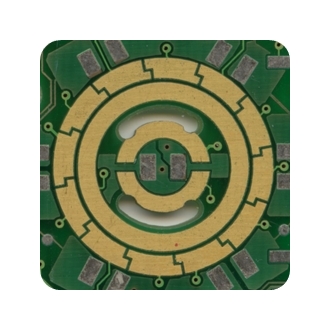
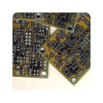
HD-Design GmbH is a service company founded in 1998 in the field of PCB layout, based in Niddatal in the Rhine-Main region. Its range of services includes schematic entry, the creation and maintenance of component libraries including 3D models according to IPC guidelines, as well as manufacturing- and EMC-optimized layout design with thermal management and, on request, impedance-controlled design. In addition, manufacturing data and documentation are produced, layouts are converted to other layout systems, and support is provided for the procurement of sample PCBs, prototypes and populated PCBs. Pulsonix and Altium Designer are used as layout systems; other systems are possible after consultation. Customers come from automotive / e-mobility, medical technology, measurement and control technology, sensor technology, and energy, control and automation technology. For projects requiring intensive coordination, especially new projects, the company also works on-site at the customer's premises.
- Site
- Niddatal
- Processes
- PCB layout, Schematic entry, Layout creation (manufacturing- and EMC-optimized, impedance-controlled on request), Component library / library work (schematic symbols, layout cells, also 3D models, according to, Data output / manufacturing data and documentation, Procurement of sample PCBs and prototypes, Support with PCB ordering, Support with PCB population / procurement of populated PCBs
- Materials
- Printed circuit board (PCB), Pulsonix, Altium Designer
- Founded
- 1998
- Industries
- Automotive / e-mobility, Medical technology, Measurement and control technology, Sensor technology, Energy, control and automation technology, Voltage monitoring / power systems
- 01
Schematic entry
- 02
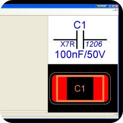
Component library (schematic symbols, layout cells, 3D models)
- 03
Layout creation (EMC- and manufacturing-optimized, thermal management, on
- 04
Data output / manufacturing data / documentation
- 05
Support with PCB ordering and population
Systems & Working Methods
Printed circuit board (PCB)
Development tool and design object of all layout services, from schematic entry to prototype procurement.
Pulsonix
Layout system used for professional PCB design projects.
Altium Designer
Layout system used; other systems are possible after consultation.
Location
Niddatal
DEHead office, PCB layout engineering services
- Lot size
- Project work / individual projects
- Materials
- Printed circuit board (PCB)
- Pulsonix
- Altium Designer
Services
Inside the production
Industries
Processes & technical limits
| Processes | Tolerance | Max. part | Weight | Lot size | Materials |
|---|---|---|---|---|---|
| PCB layoutEngineering | – | – | – | – | – |
| Schematic entryEngineering | – | – | – | – | – |
| Layout creation (manufacturing- and EMC-optimized, impedance-controlled on request)Engineering | – | – | – | – | Printed circuit board (PCB) |
| Component library / library work (schematic symbols, layout cells, also 3D models, according toEngineering | – | – | – | – | – |
| Data output / manufacturing data and documentationEngineering | – | – | – | – | – |
| Procurement of sample PCBs and prototypesEngineering | – | – | – | – | Printed circuit board (PCB) |
| Support with PCB orderingEngineering | – | – | – | – | Printed circuit board (PCB) |
| Support with PCB population / procurement of populated PCBsAssembly | – | – | – | – | Printed circuit board (PCB) |
| Conversion of existing layouts to other layout systemsEngineering | – | – | – | – | – |
| Impedance-controlled layout (as needed)Engineering | – | – | – | – | – |
Additional services
History
- 1998
Company founded; services in the field of PCB layout
- o. J.
Relocation to the new site at Freiherr-vom-Stein-Str. 7, 61194 Niddatal