
Develops and manufactures laser lithography, maskless aligner and nanofabrication systems for micro- and nanostructuring.

Heidelberg Instruments Mikrotechnik GmbH
HeidelbergNew on Amplifa
About Heidelberg Instruments
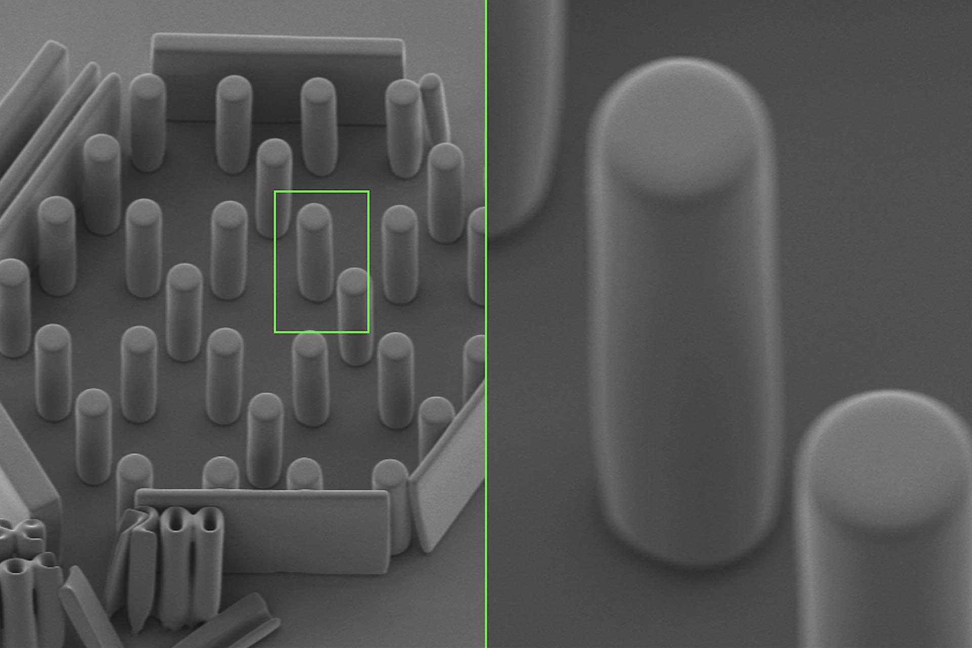
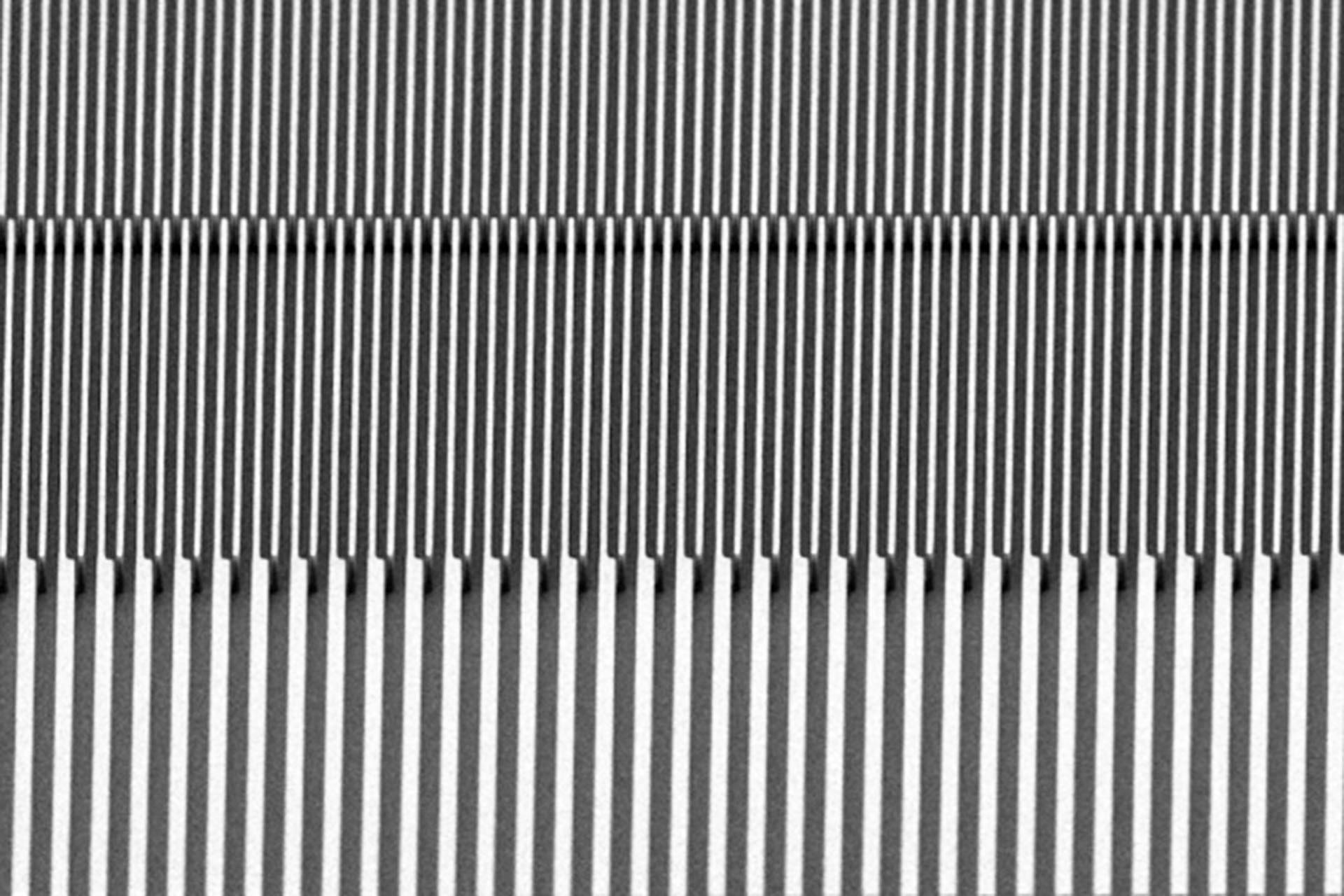
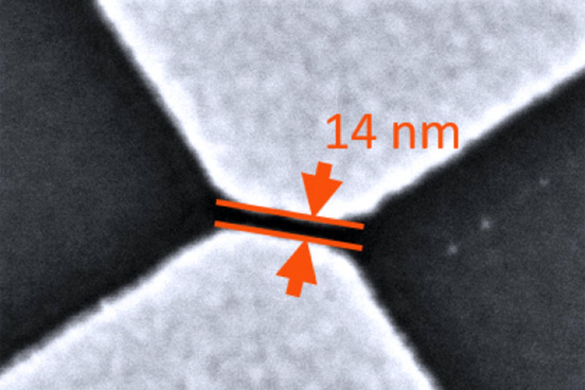
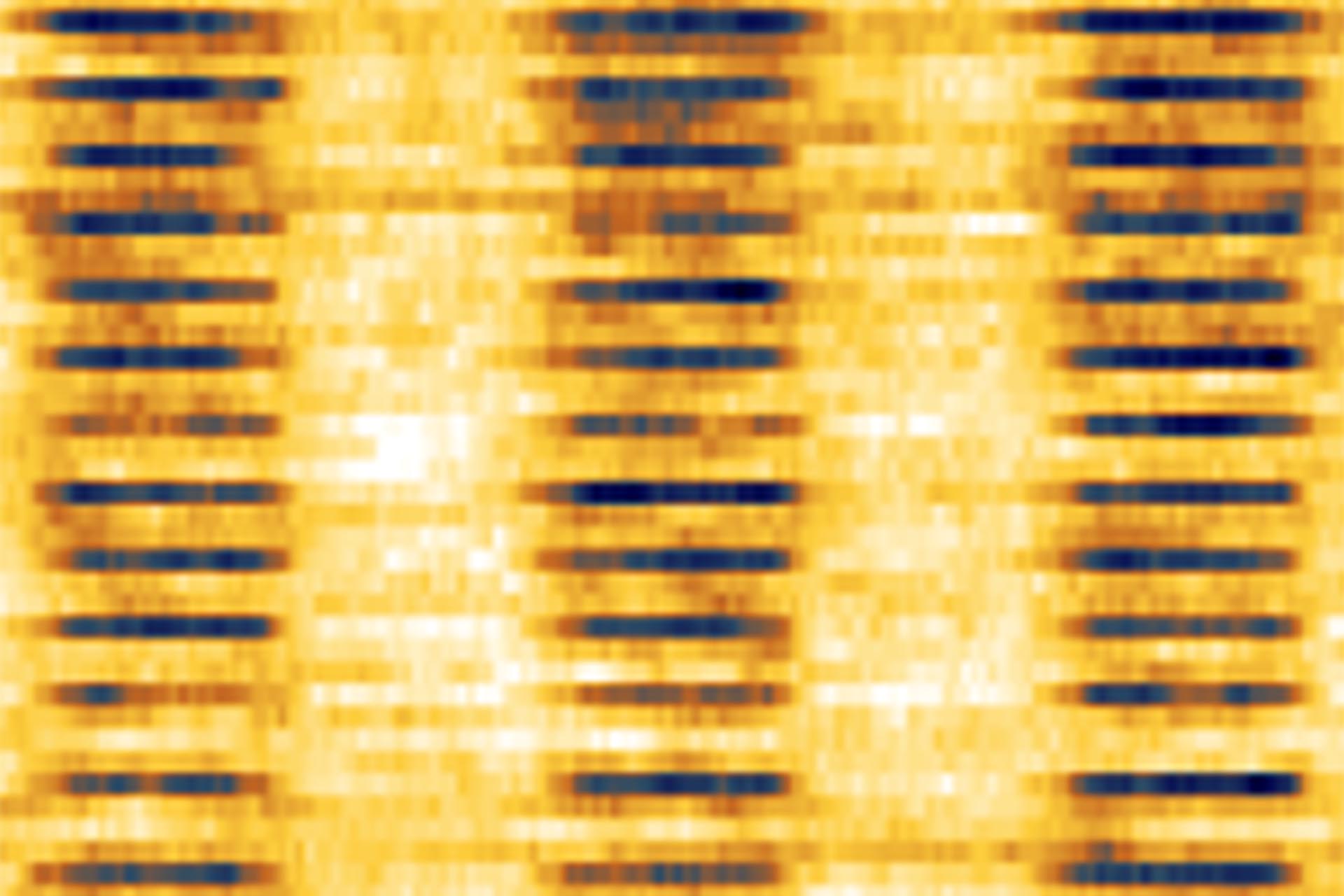
Heidelberg Instruments is a manufacturer of high-precision laser lithography systems, maskless aligners and nanofabrication tools based in Heidelberg. The portfolio ranges from compact tabletop systems for prototyping and research to production-grade equipment for photomask engineering and high-volume industrial manufacturing. The systems enable 2D and 2.5D structuring including grayscale lithography with 65,536 gray levels, direct-write lithography without masks, thermal scanning probe lithography, and single-step 3D patterning in negative resists. Dense photoresists such as SU-8 with layer thicknesses up to 800 µm are exposed in a single step, with aspect ratios up to 40:1; the optical resolution reaches down to 200 nm, and thermal scanning probe lithography down to 15 nm isolated feature size. Customers include companies, universities and research institutes, among others in micro-optics, photonics, semiconductors, advanced packaging, MEMS, microfluidics, quantum devices and biotechnology. Over 1,500 systems are installed worldwide; training and process support are offered at the Process and Application Labs (PAL) in Germany, Switzerland and China.
- Site
- Heidelberg
- Processes
- Maskless Laser Lithography (direct-write lithography, 2D and 2.5D grayscale structuring), Maskless lithography for advanced packaging with 1 µm minimum feature size, High & ultra-high resolution lithography (200 nm optical, 15 nm isolated feature size), Grayscale lithography (65,536 gray levels, photoresists up to 150 µm thick), High aspect ratio microstructures in thick photoresists (aspect ratios up to 40:1, SU-8 up to, Thermal Scanning Probe Lithography, Single-step 3D patterning of negative resists via maskless aligner (double-reentrant structures,, Photomask manufacturing for high-volume industrial production
- Materials
- SU-8, PPA Resist, AZ 125nXT, AZ 9260, mr-DWL 40, AZ nLoF 2070, Silicon, Gold
- 01
Development of the lithography systems
- 02
Manufacturing and assembly of the systems
- 03
Site Acceptance Testing at the customer
- 04
Training and support at Process and Application Labs
- 05
Application and process support
Materials and Processes
SU-8
Negative resist for high-aspect-ratio microstructures with layer thicknesses up to 800 µm in a single exposure.
AZ 125nXT
Thick negative resist for high-aspect-ratio test structures (110 µm).
AZ 9260
Positive resist for lines and structures in the thick-film range (e.g. 10 µm).
AZ nLoF 2070
i-Line negative resist for lift-off and single-step 3D patterning.
mr-DWL 40
Negative resist for microfluidic channels and lattice structures with overhanging features.
PPA Resist
Thermosensitive resist for thermal scanning probe lithography with resolution down to 15 nm.
Silicon
Functional substrate for pattern transfer via reactive ion etching.
Gold
Metal film for pattern transfer via ion beam etching, e.g. for plasmonic applications.
Chromium
Material for photomasks into which structures are etched.
Silicon dioxide
Material for defined ellipses in the high-resolution lift-off process.
Aluminum oxide
Material for nanopoints in the high-resolution lift-off process.
Locations
Heidelberg
DEHeadquarters and system development
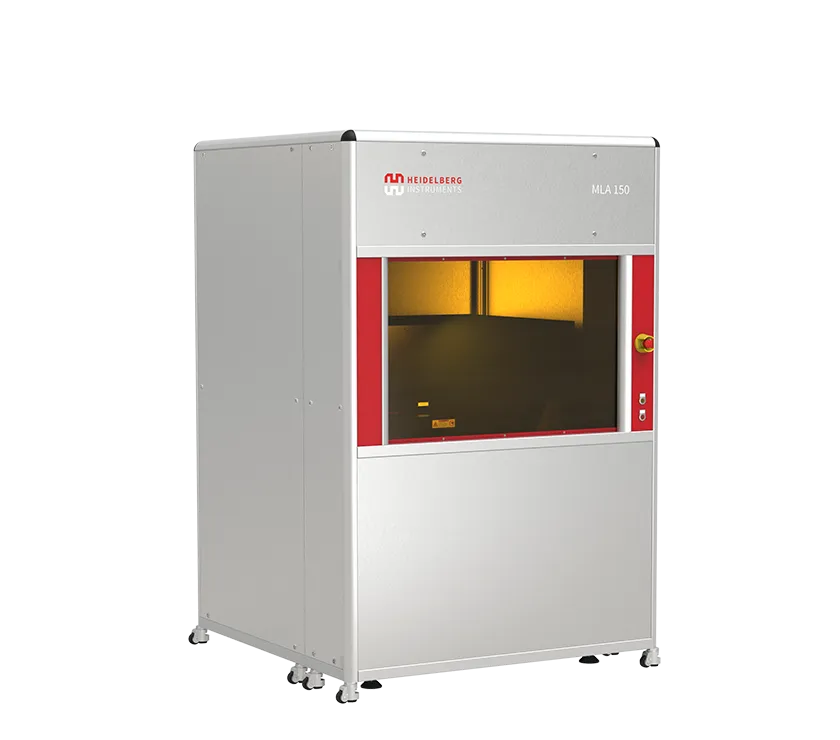
- Maskless Aligner MLA 150
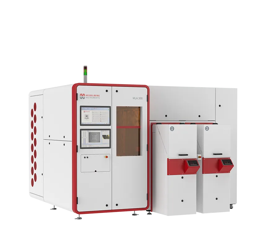
- Maskless Aligner MLA 300
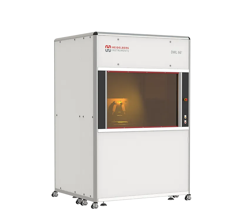
- Laser Lithography System DWL 66+
- NanoFrazor Thermal Scanning Probe Lithography
- Direct Imager VPG 300 DI
- Volume Pattern Generator VPG+ 800
- DWL 4000 GS
- VPG+ 1850 FPD
Systems and Equipment
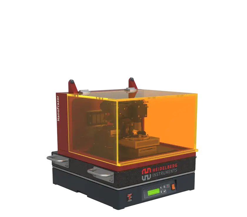
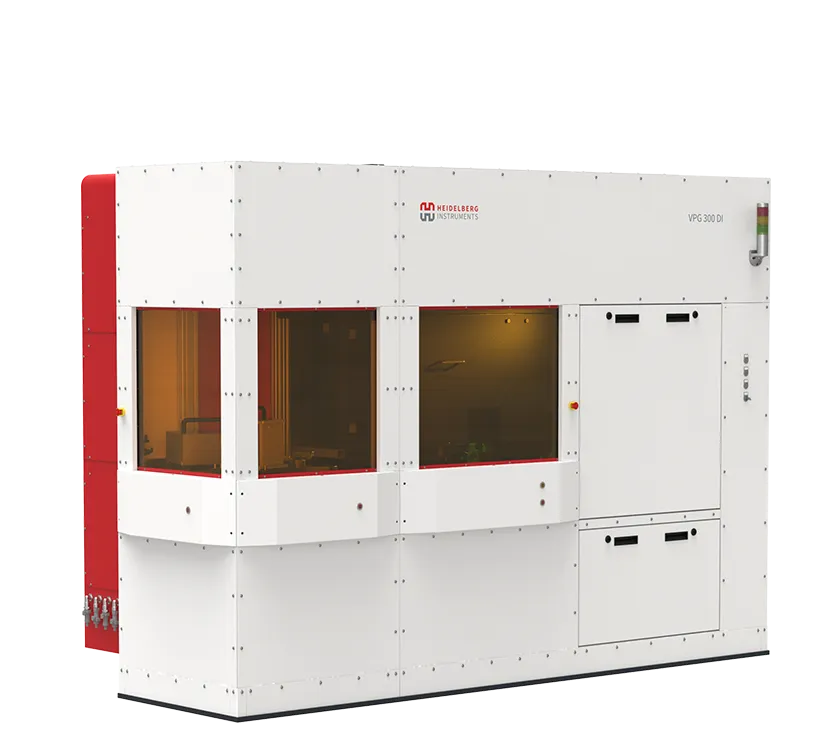
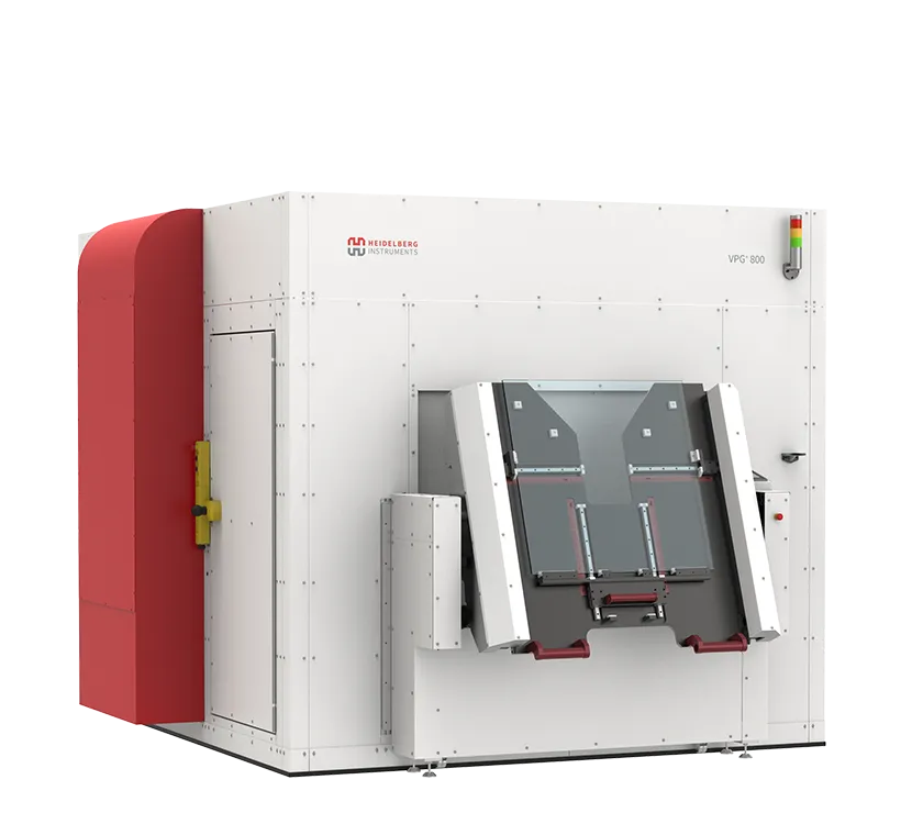
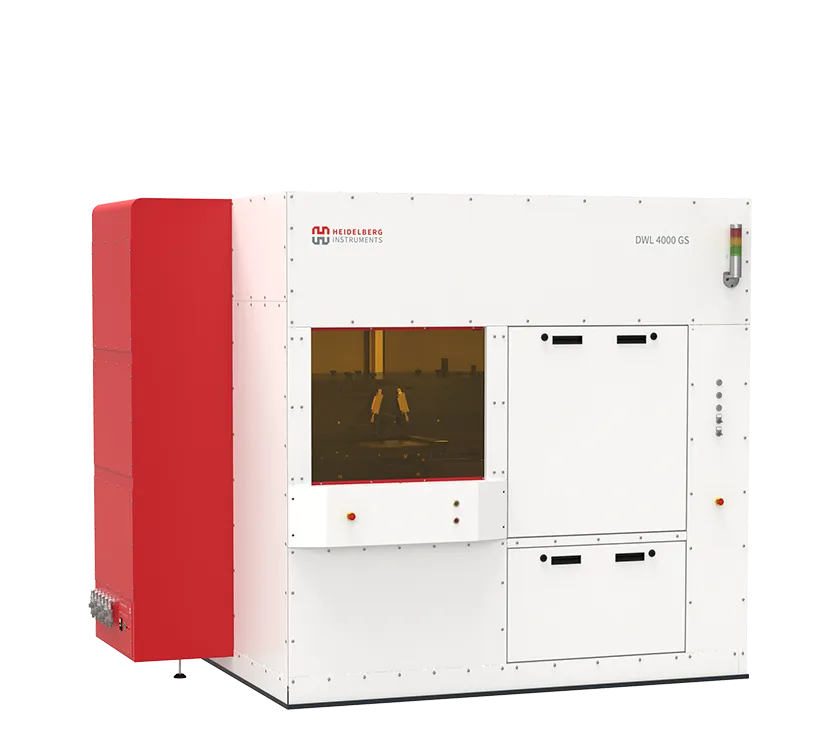
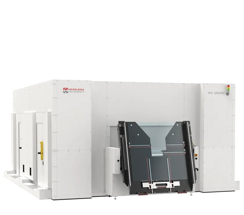
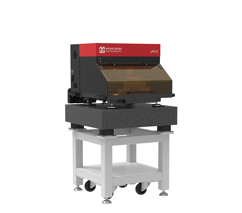
Inside the production
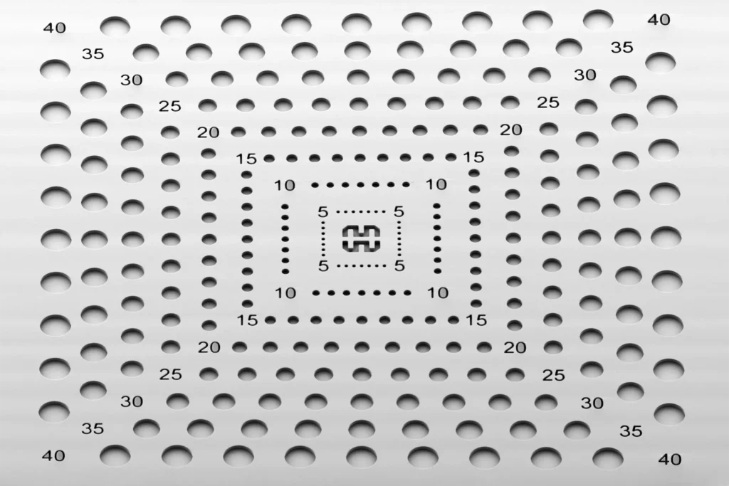
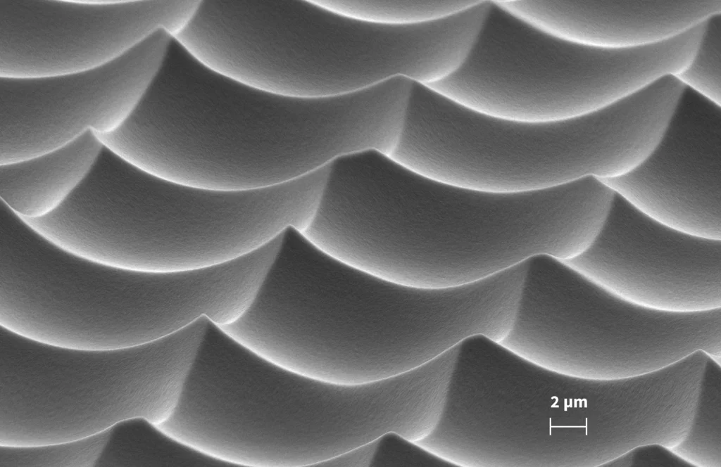
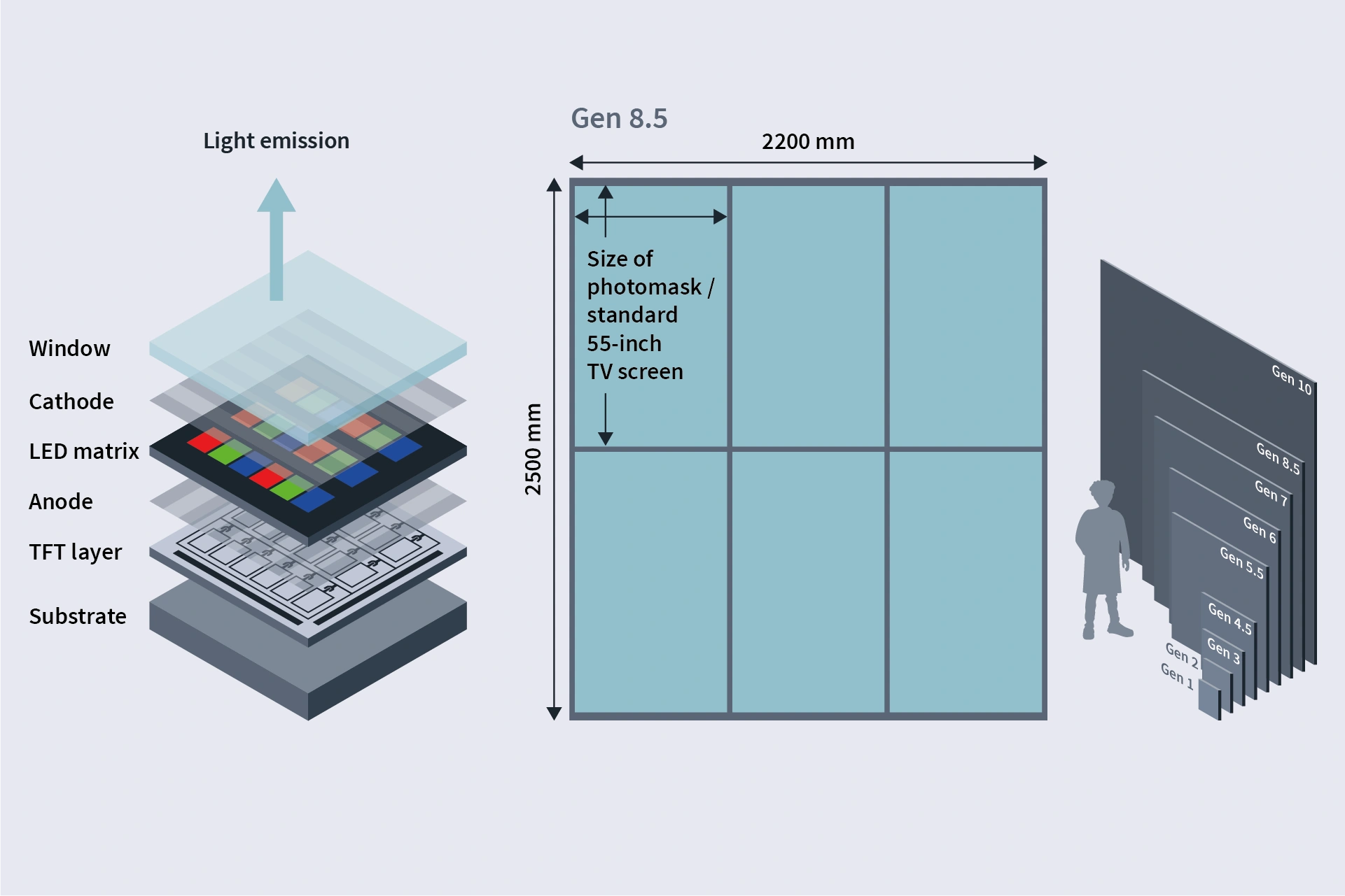
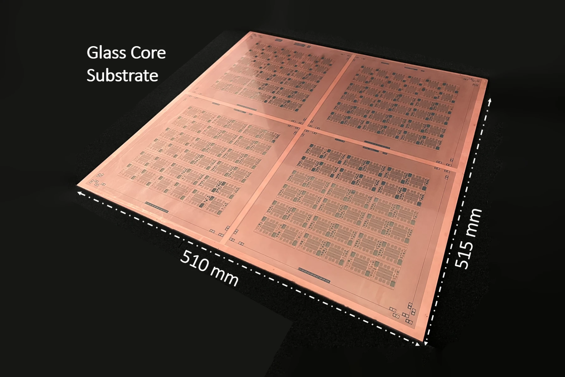
Processes & technical limits
| Processes | Tolerance | Max. part | Weight | Lot size | Materials |
|---|---|---|---|---|---|
| Maskless Laser Lithography (direct-write lithography, 2D and 2.5D grayscale structuring)Engineering | – | – | – | – | Photoresists (SU-8, PPA, AZ 125nXT, AZ 9260, mr-DWL 40, AZ, Silicon, Gold, Chromium (photomasks) |
| Maskless lithography for advanced packaging with 1 µm minimum feature sizeEngineering | – | – | – | – | – |
| High & ultra-high resolution lithography (200 nm optical, 15 nm isolated feature size)Engineering | – | – | – | – | PPA Resist, Silicon, Gold |
| Grayscale lithography (65,536 gray levels, photoresists up to 150 µm thick)Engineering | – | – | – | – | Photoresist |
| High aspect ratio microstructures in thick photoresists (aspect ratios up to 40:1, SU-8 up toEngineering | – | – | – | – | SU-8, AZ 125nXT, AZ 9260, mr-DWL 40, AZ nLoF 2070 |
| Thermal Scanning Probe LithographyEngineering | – | – | – | – | PPA |
| Single-step 3D patterning of negative resists via maskless aligner (double-reentrant structures,Engineering | – | – | – | – | mr-DWL 40, AZ nLoF 2070, SU-8, Polyimides |
| Photomask manufacturing for high-volume industrial productionEngineering | – | – | – | – | Chromium |
4 Anlagen & Maschinen
| Machine | Manufacturer / model | Quantity | Working area | Year built | Site |
|---|---|---|---|---|---|
| Maskless Aligner (laser lithography system for production) | Heidelberg Instruments MLA 300 | – | – | – | – |
| Maskless Aligner | Heidelberg Instruments MLA 150 | – | – | – | – |
| Laser lithography system (direct write) | Heidelberg Instruments DWL 66+ | – | – | – | – |
| Thermal Scanning Probe Lithography System | Heidelberg Instruments Nano NanoFrazor | – | – | – | – |
Additional services
Reference customers
History
Over 40 years of experience in micro- and nanofabrication; more than 1,500 systems installed worldwide.