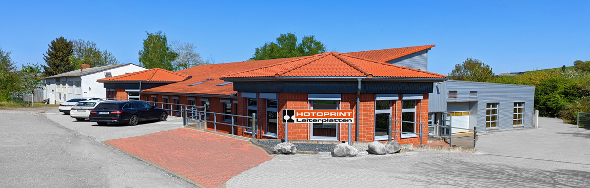
German PCB manufacturing: multilayers up to 12 layers, flex, rigid-flex, IMS and RFID printed circuit boards including prototypes from 3 working days.

HOTOPRINT Elektronik GmbH & Co. KG
LamspringeNew on Amplifa
About Hotoprint
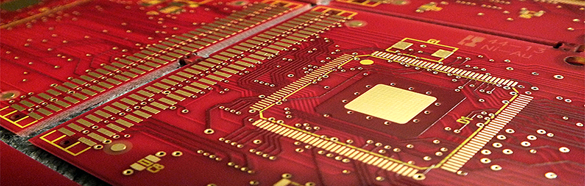
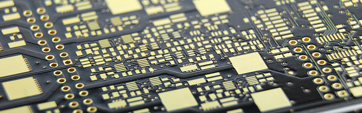
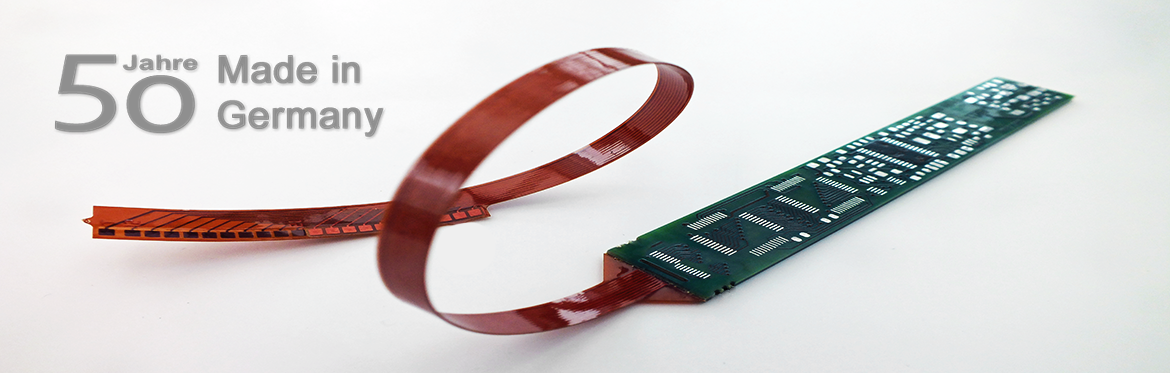
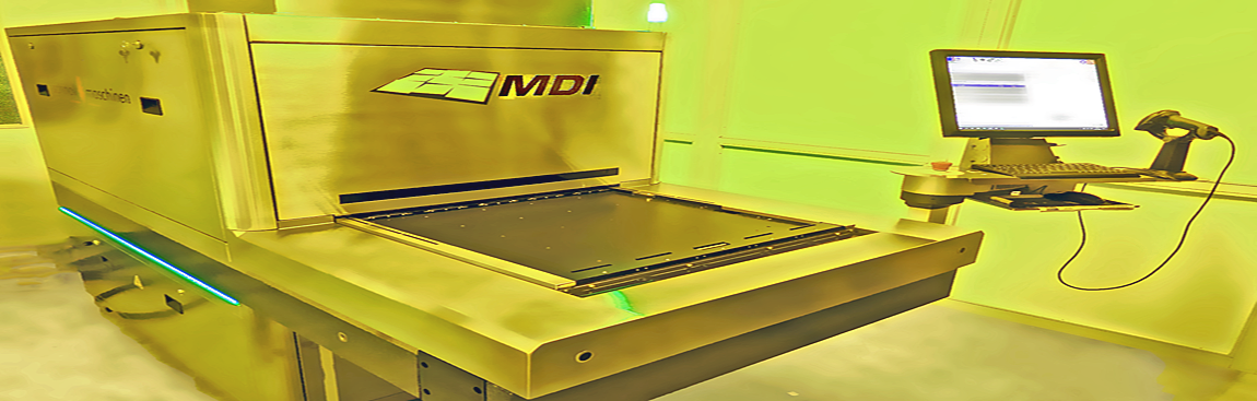
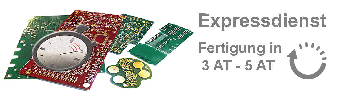
Hotoprint Elektronik is a family-owned manufacturer of high-precision printed circuit boards founded in 1974 and based in Lamspringe (Lower Saxony). Its manufacturing range covers single- and double-sided printed circuit boards, multilayers up to 12 layers, fine-line boards with micro vias, blind vias, buried vias and plugging, as well as flexible, rigid-flex and semiflex boards on a polyimide basis. In addition, IMS boards with an aluminium core and boards with an integrated RFID module for traceability and anti-counterfeiting are manufactured. The entire value chain takes place in Germany – from CAD/CAM via MDI direct imaging with UV-LED, drilling, electroplating, solder mask coating and surface finishing through to milling, screen printing, AOI inspection and electrical testing. Surface finishes include hot-air leveling, chemical tin and nickel-palladium-gold. Prototypes and express services are deliverable from 3 working days; the standard lead time for double-/multilayer boards is currently 10 working days.
- Site
- Lamspringe
- Processes
- Single-sided printed circuit boards, Double-sided printed circuit boards, Multilayers up to 12 layers, Micro vias / blind vias / buried vias / plugging, Flexible printed circuit boards, Rigid-flex & semiflex printed circuit boards, IMS boards (aluminium core), Printed circuit boards with integrated RFID module
- Materials
- Copper, FR4, Polyimide, Aluminium (aluminium core), Tin (chemical), Nickel-Palladium-Gold, Chemical tin, Hot-Air-Leveling
- Certificates
- DIN ISO 9001:2015, ISO 9001
- Founded
- 1974
- Industries
- Electronics
- 01
CAD/CAM
- 02
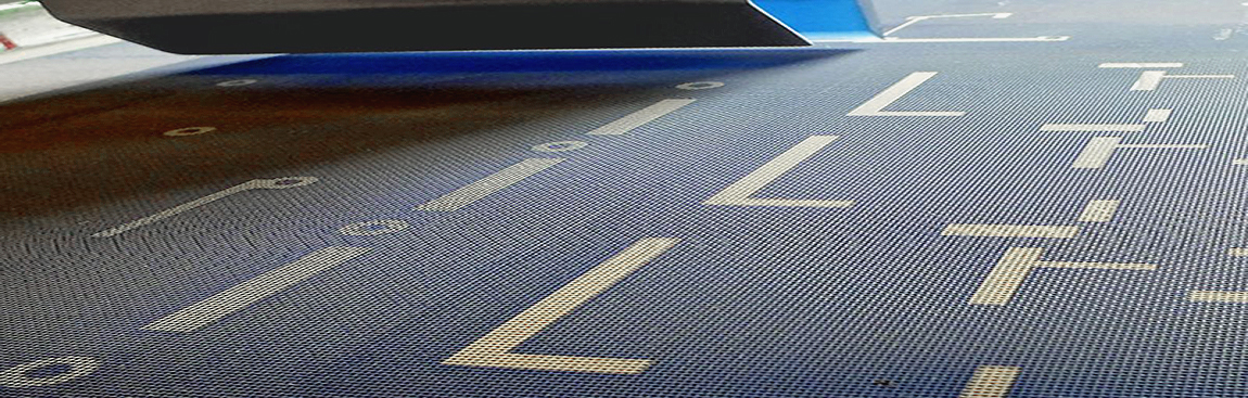
MDI direct imaging (circuit pattern)
- 03
Drilling
- 04
Desmear/shadow process
- 05
Electroplating
- 06
Stripping/etching
- 07
Solder mask coating
- 08
Surface finishing
- 09
Screen printing
- 10
Milling
- 11
AOI inspection
- 12
Electrical testing
Materials & Processes
FR4
Standard base material for single- and double-sided printed circuit boards as well as multilayers.
Polyimide
Base material for flexible as well as rigid-flex and semiflex printed circuit boards.
Aluminium (aluminium core)
Core material for IMS boards with improved heat dissipation.
Copper
Conductor material for all board types, also in electroplating.
Chemical tin
Surface finish as a solder-friendly finish.
Nickel-Palladium-Gold
Surface finish for the highest requirements on contact reliability.
Hot-Air-Leveling
Proven hot-air finishing process for printed circuit board surfaces.
Sites
Lamspringe
DEManufacturing / Headquarters
- Lot size
- Prototypes to series (lot size from 1)
- Materials
- FR4, polyimide, aluminium, copper
- Electroplating line
- CNC drilling/milling machines
- MDI direct imaging with UV-LED
Components
Inside the production

Industries
Processes & technical limits
| Processes | Tolerance | Max. part | Weight | Lot size | Materials |
|---|---|---|---|---|---|
| Single-sided printed circuit boardsPCB manufacturing | – | – | – | – | Copper, FR4 |
| Double-sided printed circuit boardsPCB manufacturing | – | – | – | – | Copper, FR4 |
| Multilayers up to 12 layersPCB manufacturing | – | – | – | – | Copper, FR4 |
| Micro vias / blind vias / buried vias / pluggingPCB manufacturing | – | – | – | – | – |
| Flexible printed circuit boardsPCB manufacturing | – | – | – | – | Polyimide, Copper |
| Rigid-flex & semiflex printed circuit boardsPCB manufacturing | – | – | – | – | Polyimide, Copper, FR4 |
| IMS boards (aluminium core)PCB manufacturing | – | – | – | – | Aluminium, Copper |
| Printed circuit boards with integrated RFID modulePCB manufacturing | – | – | – | – | – |
| Prototypes & express service (from 3 working days)PCB manufacturing | – | – | – | 1 | – |
| Multilayer pressing/laminationPCB manufacturing | – | – | – | – | – |
| DrillingPCB manufacturing | – | – | – | – | – |
| Desmear / shadow processPCB manufacturing | – | – | – | – | – |
| Photolithography – circuit pattern (MDI direct imaging with UV-LED)PCB manufacturing | – | – | – | – | – |
| ElectroplatingSurface | – | – | – | – | Copper |
| Stripping / etchingPCB manufacturing | – | – | – | – | Copper |
| Optical inspection / AOITesting | – | – | – | – | – |
| Solder mask coatingSurface | – | – | – | – | – |
| Surface finishing (hot-air leveling, chemical tin, nickel-palladium-gold)Surface | – | – | – | – | Tin, Nickel, Palladium, Gold |
| MillingPCB manufacturing | – | – | – | – | FR4, Aluminium, Polyimide |
| Screen printingSurface | – | – | – | – | – |
| Electrical testingTesting | – | – | – | – | – |
| CAD / CAMEngineering | – | – | – | – | – |
| Direct printing and integration of optical short-range networksPCB manufacturing | – | – | – | – | – |
3 Anlagen & Maschinen
| Machine | Manufacturer / model | Quantity | Working area | Year built | Site |
|---|---|---|---|---|---|
| Electroplating line | – | – | – | – | Lamspringe |
| CNC drilling/milling machines | – | – | – | – | Lamspringe |
| MDI direct imaging with UV-LED | – | – | – | – | Lamspringe |
Additional services
Quality
PCB manufacturing is safeguarded by AOI inspection and electrical testing. The company is re-certified according to DIN ISO 9001:2015.
| Evidence | Lamspringe |
|---|---|
| ISO 9001 |
History
- 1974
Company founded; over 50 years of experience in PCB manufacturing.