
Development and manufacture of liquid photoresists and photopolymer coatings for etching, electroforming and PCB applications.
HTP HiTech Photopolymere AG
Basel (CH)New on Amplifa
About HTP HiTech Photopolymere AG
HTP HiTech Photopolymere AG is a manufacturer based in Basel specializing in photopolymers. Founded in 1997 by three former CIBA-Geigy experts, the company develops and manufactures custom photopolymer coatings and liquid photoresists for etching and electroforming applications. The company's origins lie in photoresists for the inner layers of multilayer printed circuit boards (PCB); over the years HTP expanded its portfolio to include engraving technologies, Photochemical Machining (PCM), security features and specialty coatings. The photoresists are predominantly applied by dip coating, with spray and roller coating also possible depending on the customer's equipment. In addition to product supply, HTP offers technical consulting, process optimization and troubleshooting for photoresists, coating technologies and wet chemistry, as well as contract research & development from laboratory formulation to production batches. In addition, the company supplies processing chemicals for photochemical processes and provides contract manufacturing, warehousing and logistics for customers worldwide.
- Site
- Basel
- Processes
- Manufacture of liquid photopolymer coatings and liquid photoresists for etching and, Photoresist application by dip coating, Photoresist application by spray coating, Photoresist application by roller coating, Photochemical Machining (PCM) – process development and product supply for photo-etching, Products and process know-how for printed circuit board manufacturing (PCB/PWB, photoresists for, Specialty Coatings & Security Applications, Processing chemicals for photochemical processes
- Materials
- Metals (broad range, not specified), Liquid Photoresists (Liquid Photoresists), Dip Coating (Dip-Coating), Spray Coating (Spray-Coating), Roller Coating (Roller-Coating), Specialty Coatings (Specialty Coatings), Processing Chemicals (Processing Chemicals)
- Founded
- 1997
- Industries
- Photochemical Machining (PCM), Printed circuit board manufacturing (PCB), Specialty Coatings, Security, Printed Circuit Boards (PCB)/Circuit boards, Security Applications
- 01
R&D and custom resist formulation
- 02
Production of the liquid photopolymers/photoresists
- 03
Application by dip, spray or roller coating
- 04
Process integration, consulting and troubleshooting at the customer
- 05
Warehousing and logistics
Products, Materials & Processes
Liquid Photoresists (Liquid Photoresists)
For etching and electroforming applications for high-precision metal microstructuring, primarily for PCB inner layers and PCM.
Dip Coating (Dip-Coating)
Main application method of HTP photoresists on metal substrates.
Spray Coating (Spray-Coating)
Optional application method depending on the customer's equipment setup.
Roller Coating (Roller-Coating)
Optional application method for industrial coating systems.
Specialty Coatings (Specialty Coatings)
Photopolymer coatings designed for durability, adhesion and functional performance.
Processing Chemicals (Processing Chemicals)
Wet-chemical products for photochemical processes in PCM and PCB.
Locations

Basel
CHHeadquarters, development and production
- Lot size
- Lab to production batches
- Materials
- Liquid photoresists, specialty coatings, processing chemicals
Applications & Components


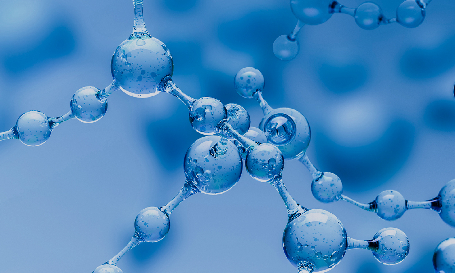
Inside the production



Industries
Processes & technical limits
| Processes | Tolerance | Max. part | Weight | Lot size | Materials |
|---|---|---|---|---|---|
| Manufacture of liquid photopolymer coatings and liquid photoresists for etching andSurface | – | – | – | Production from pilot to full scale | Metals (further range not specified) |
| Photoresist application by dip coatingSurface | – | – | – | – | Metals |
| Photoresist application by spray coatingSurface | – | – | – | – | Metals |
| Photoresist application by roller coatingSurface | – | – | – | – | Metals |
| Photochemical Machining (PCM) – process development and product supply for photo-etchingSurface | – | – | – | – | Metals |
| Products and process know-how for printed circuit board manufacturing (PCB/PWB, photoresists forSurface | – | – | – | – | – |
| Specialty Coatings & Security ApplicationsSurface | – | – | – | – | – |
| Processing chemicals for photochemical processesSurface | – | – | – | – | – |
| Contract manufacturing/contract coating as a serviceSurface | – | – | – | – | – |
| Technical consulting, process optimization and troubleshooting for photoresists,Engineering | – | – | – | – | – |
| Contract research & development: custom resist formulation, laboratory testing, production fromEngineering | – | – | – | lab-scale – full scale batch sizes | – |
| Engraving/exposure technologies (engraving technologies)Surface | – | – | – | – | – |
Additional services
History
- 1997
Founded by three former CIBA-Geigy experts (Dr. Kurt Meier, Charles Gantner, Diethard Kapp-Schwoerer); started with photoresists for inner layers of multilayer printed circuit boards.
- 2025
A new chapter under a renewed management team led by CEO Dr. David Schwärzle; founders Kurt Meier and Diethard Kapp-Schwoerer remain owners and strategic advisors.