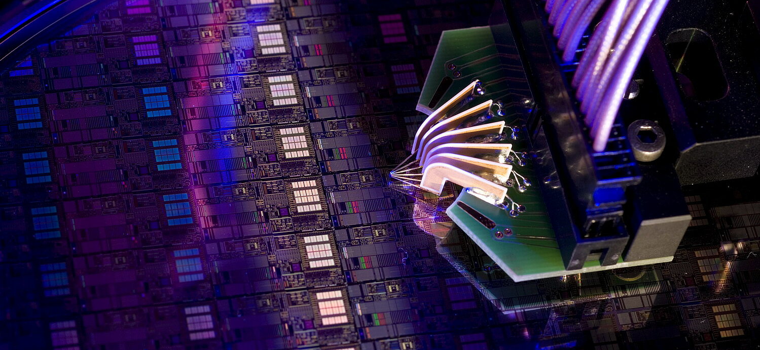
ASIC manufacturing in SiGe BiCMOS technology: foundry services, packaging and metrology for industry and research

IHP Solutions GmbH
Frankfurt (Oder), GermanyNew on Amplifa
About IHP Solutions
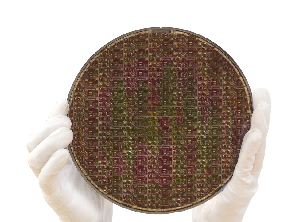
IHP Solutions GmbH is the commercialization and technology transfer company of the Leibniz Institute for Innovative Microelectronics (IHP) in Frankfurt (Oder), founded in 2015. The company transfers the institute's semiconductor technology to industrial customers and research institutions worldwide. Its core offering is foundry services for application-specific integrated circuits (ASICs) in SiGe BiCMOS technology at 0.25 µm and 0.13 µm on 200-mm wafers, including integrated RF modules and silicon photonics. Chip fabrication takes place in IHP's 1500 m² cleanroom fab (Class 3) operating 24/7 – from prototyping through multi-project wafer and engineering runs to low volume production. In addition, IHP Solutions offers packaging and value added services (grinding, dicing, sorting, advanced packaging, PCB assembly), metrology and test services, IC design services, and IP licensing. Customers are primarily found in RF/microwave technology, wireless communication in higher GHz bands, radar, and silicon photonics. Representatives are based in the USA (Americas/Japan) and in Hong Kong (China/Hong Kong/Taiwan).
- Site
- Frankfurt (Oder)
- Processes
- SiGe BiCMOS chip production (MPW runs, 40 ICs per run), Engineering runs (custom production, 6 wafers), Low Volume Production (LVP), Wafer grinding (thinning) 200/300 µm, TAIKO down to 50 µm, Blade dicing, Laser dicing, Stealth dicing, Dicing before grinding
- Materials
- Silicon, SiGe (silicon-germanium), Copper, Solder (solder balls), SiGe BiCMOS technology (0.25 µm and 0.13 µm), Silicon (200-mm wafers), Silicon photonics on SOI wafers, TSV (through-silicon vias)
- Certificates
- Measurement & test support (device, functional, analog/RF, digital), Automatic optical inspection (AOI 2D/3D, 0.25 µm/pixel), ISO 9001
- Founded
- 2015
- Employees
- < 500 (small
- Industries
- Microelectronics / semiconductor (ASIC manufacturing), RF and microwave technology / radar, Wireless communication (higher GHz bands), Silicon photonics, Research institutions and universities, Microelectronics/semiconductor (ASIC manufacturing)
- 01
IC design and design services (Cadence, ADS)
- 02
Mask/wafer production (MPW, engineering runs)
- 03
Low Volume Production
- 04
Wafer grinding / thinning
- 05
Dicing (blade, laser, stealth)
- 06
AOI inspection
- 07
Die sorting and packaging
- 08
Advanced packaging (RDL, solder balls, flip chip, bonding)
- 09
PCB assembly
- 10
Measurement & test support
Technologies and Processes
SiGe BiCMOS technology (0.25 µm and 0.13 µm)
Semiconductor process with integrated HBTs with cutoff frequencies up to 500 GHz for RF and radar applications.
Silicon (200-mm wafers)
Substrate material of chip fabrication, optionally as SOI wafers for photonic design layers.
Silicon photonics on SOI wafers
Additional photonic design layers combined with BiCMOS BEOL layers for integrated photonic ICs.
TSV (through-silicon vias)
Option in SG13S/SG13G2 for RF grounding through vias through the silicon.
Localized backside etching
Local etching of silicon on the wafer backside to improve passive devices.
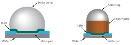
Copper (RDL, copper pillars)
Material for redistribution layers and copper pillars in advanced packaging.
Solder (solder balls)
Material for bump metallization and flip-chip assembly.
Location
Frankfurt (Oder)
DEHeadquarters; IHP SiGe BiCMOS pilot fab (cleanroom, prototyping, LVP, packaging, metrology)
- Lot size
- MPW runs (40 ICs per run), engineering runs (6 wafers), low volume production
- Materials
- Silicon, SiGe (BiCMOS 0.25 µm and 0.13 µm)
- SiGe BiCMOS wafer fab (200 mm, 0.13 µm), 1500 m² Class 3 cleanroom, 24/7 operation
- AOI inspection system 2D/3D, max. 0.25 µm/pixel
- Grinding up to 12" (150–750 µm, TAIKO down to 50 µm)
- Dicing: blade, laser, stealth, dicing before grinding
- Die sorting & packaging (waffle pack, vacuum release tray, gel pack, tape)
- Advanced packaging: RDL, solder balls, copper pillars, flip chip, chip on board, die/wire bonding
- PCB assembly
- Measurement and test equipment (device/functional/RF/digital)
Components and Services
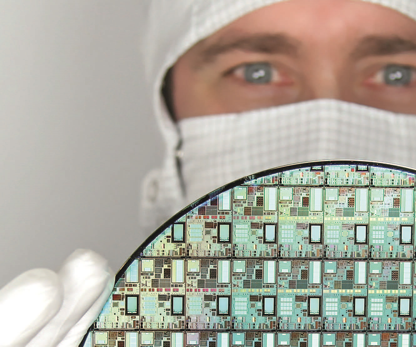
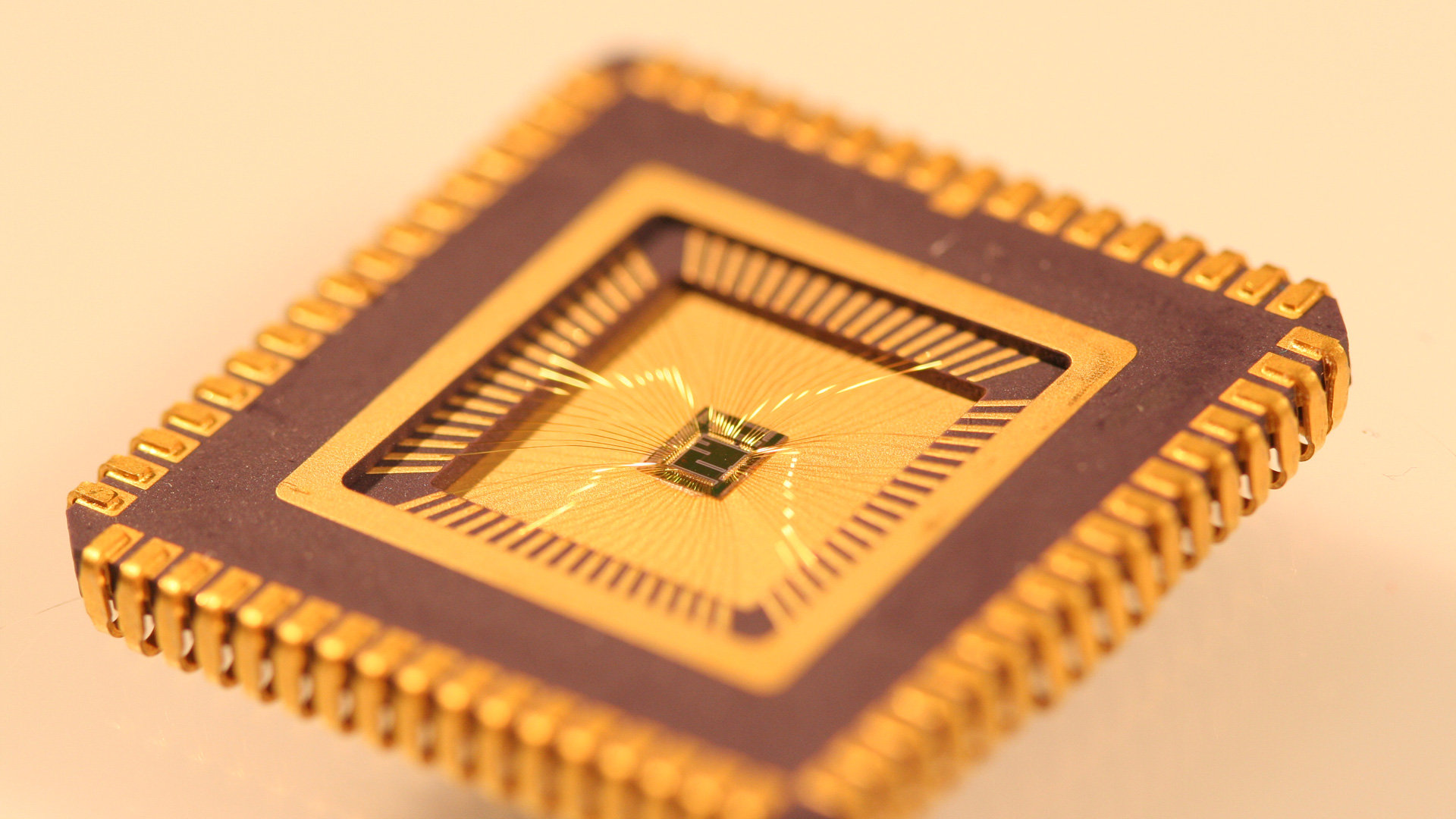
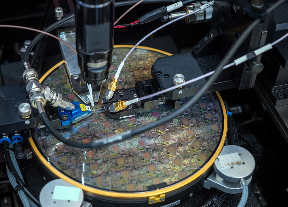
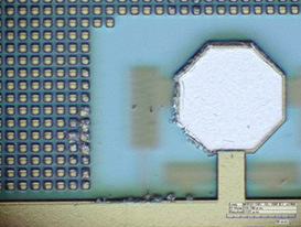
Inside the production

Industries
Processes & technical limits
| Processes | Tolerance | Max. part | Weight | Lot size | Materials |
|---|---|---|---|---|---|
| SiGe BiCMOS chip production (MPW runs, 40 ICs per run)Semiconductor manufacturing | – | 200 mm (wafer) | – | 40 ICs | Silicon, SiGe |
| Engineering runs (custom production, 6 wafers)Semiconductor manufacturing | – | 200 mm (wafer) | – | 6 wafers | Silicon, SiGe |
| Low Volume Production (LVP)Semiconductor manufacturing | – | 200 mm (wafer) | – | – | Silicon, SiGe |
| Wafer grinding (thinning) 200/300 µm, TAIKO down to 50 µmSurface and thin-film technology | – | 12" (wafer) | – | – | Silicon |
| Blade dicingCutting/separating | – | 12" (wafer) | – | – | Silicon |
| Laser dicingCutting/separating | – | 12" (wafer) | – | – | Silicon |
| Stealth dicingCutting/separating | – | 12" (wafer) | – | – | Silicon |
| Dicing before grindingCutting/separating | – | 12" (wafer) | – | – | Silicon |
| Automatic optical inspection (AOI), 2D/3D, max. 0.25 µm/pixelTesting/inspection | – | – | – | – | Silicon |
| Die sorting and packaging (waffle pack, vacuum release tray, gel pack, tape)Handling/packaging | – | – | – | – | – |
| PCB assemblyAssembly | – | – | – | – | Copper |
| Redistribution layer (RDL)Packaging/interconnection technology | – | – | – | – | Copper |
| Solder ball placementPackaging/interconnection technology | – | – | – | – | Solder, Copper |
| Copper pillar placementPackaging/interconnection technology | – | – | – | – | Copper |
| Flip chipPackaging/interconnection technology | – | – | – | – | – |
| Chip on boardPackaging/interconnection technology | – | – | – | – | – |
| Die bondingPackaging/interconnection technology | – | – | – | – | – |
| Wire bondingPackaging/interconnection technology | – | – | – | – | – |
| On-wafer measurements (device/functional/RF/digital)Testing/inspection | – | 200 mm (wafer) | – | – | – |
| IC design services / PCB designEngineering/design | – | – | – | – | – |
2 Anlagen & Maschinen
| Machine | Manufacturer / model | Quantity | Working area | Year built | Site |
|---|---|---|---|---|---|
| SiGe BiCMOS pilot foundry (wafer fab) | IHP | – | 1500 m² Class 3 cleanroom, 200 mm wafers, 0.13 µm technology | – | Frankfurt (Oder) |
| AOI inspection system (2D/3D) | – | – | Max. resolution 0.25 µm/pixel | – | Frankfurt (Oder) |
Additional services
Quality and Metrology
IHP Solutions offers access to IHP's full measurement and test equipment, including automatic optical inspection (AOI, 2D/3D) with a maximum resolution of 0.25 µm/pixel as well as device, functional, analog/RF and digital measurements. Manufacturing and packaging take place in a 1500 m² Class 3 cleanroom in 24/7 operation.
| Evidence | Frankfurt (Oder) |
|---|---|
| Measurement & test support (device, functional, analog/RF, digital) | |
| Automatic optical inspection (AOI 2D/3D, 0.25 µm/pixel) | |
| ISO 9001 |
History
- 2015
Foundation of IHP Solutions GmbH as the commercialization and technology transfer company of the Leibniz Institute for Innovative Microelectronics (IHP).
- 2022
Mirtha Valenzuela Vera becomes sole managing director on 15.11.2022.