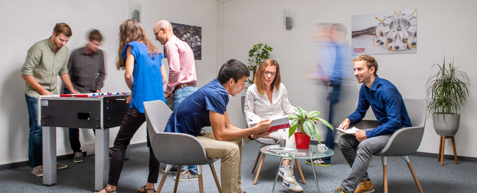
High-precision robotics and probing solutions for microscopy and semiconductor analysis.

Imina Technologies SA
Switzerland (Headquarters)New on Amplifa
About Imina Technologies
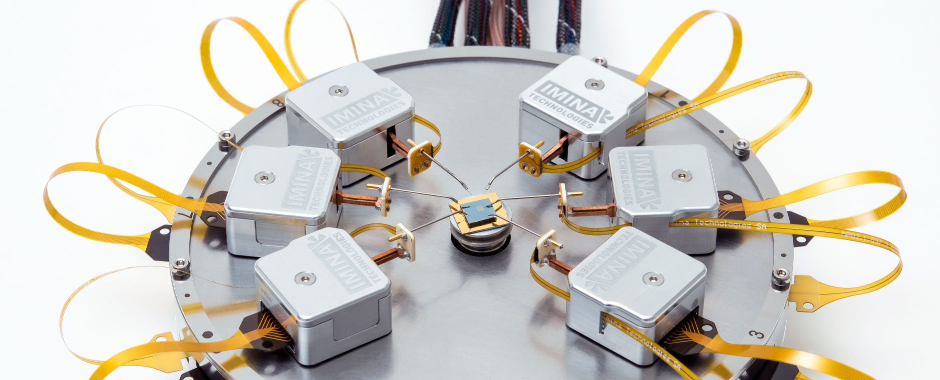
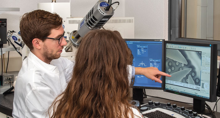
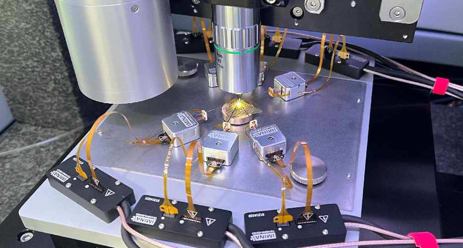
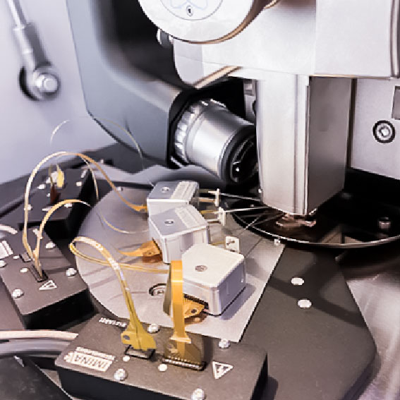
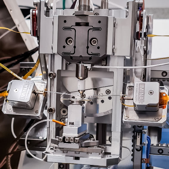
Imina Technologies SA is a company founded in Switzerland in 2009, emerging from more than ten years of research at the robotics laboratory of EPFL. The company develops and manufactures high-precision robotics solutions for microscopes, enabling samples of integrated circuits, wafers, MEMS and nanowires to be positioned, contacted and electrically characterized down to the nanometer scale. The miBot™ product family comprises the NANO product line for in-situ nanoprobing and electrical failure analysis in scanning electron microscopes (SEM, FIB, Dual Beam) as well as the MICRO product line for optical microscopes, probe stations and inspection tools; the Precisio™ software controls measurement sequences, recipe management and reporting. In addition to its product range, the company offers engineering services for mechanical, electrical and software integration into third-party equipment, nanoprobing and EFA services including sample preparation, as well as installation, training and support. Customers include leading semiconductor manufacturers and renowned research institutes worldwide; sales are conducted internationally through a partner network.
- Site
- Switzerland (Headquarters)
- Processes
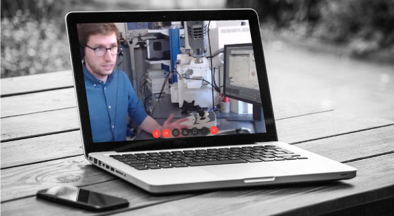
- Nanoprobing and electrical failure analysis (EFA) as a service incl. sample preparation, Engineering services: mechanical, electrical and software integration of, Installation, training, online coaching, site acceptance tests, SWAP program, Engineering services (mechanical, electrical and software integration), Installation and advanced training, Online coaching, Site acceptance tests, SWAP program (replacement system within 3 business days)
- Materials
- Semiconductors (integrated circuits, wafers, MEMS, nanowires), Integrated Circuits, Wafers, MEMS, Nanowires
- Certificates
- Site Acceptance Tests, Feasibility studies in the application laboratory, SWAP program (replacement system within 3 business days)
- Founded
- 2009
- Industries
- Semiconductor industry, Micro- and nanotechnology, Failure Analysis, Materials research / Research institutes
- 01
Research & Development
- 02
Mechanical, electrical and software integration
- 03
Installation & Training
- 04
Site Acceptance Tests
- 05
Support & SWAP program
- 06
Nanoprobing/EFA services
Samples & Measurement Objects
Integrated Circuits
Electrical characterization of semiconductor devices at the smallest technology nodes.
Wafers
Probing and failure analysis of semiconductor wafers.
MEMS
Manipulation and characterization of MEMS structures.
Nanowires
Isolation of individual particles and testing of nanowires down to the nanometer scale.
Locations
Switzerland (Headquarters)
CHHeadquarters, development, application laboratory and services
- Materials
- Semiconductor devices (ICs, wafers, MEMS, nanowires)
- miBot™ nanoprobing systems (NANO Line)
- miBot™ microprobing systems (MICRO Line)
- Precisio™ software
Products & Solutions
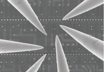
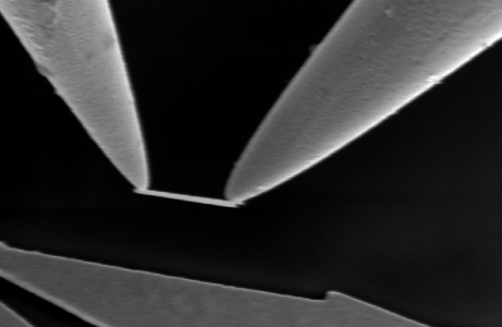
Inside the production
Industries
Processes & technical limits
| Processes | Tolerance | Max. part | Weight | Lot size | Materials |
|---|---|---|---|---|---|
| Nanoprobing and electrical failure analysis (EFA) as a service incl. sample preparationTesting | – | – | – | – | Semiconductor devices (ICs, wafers, MEMS, nanowires) |
| Engineering services: mechanical, electrical and software integration ofEngineering | – | – | – | – | – |
| Installation, training, online coaching, site acceptance tests, SWAP programEngineering | – | – | – | – | – |
5 Anlagen & Maschinen
| Machine | Manufacturer / model | Quantity | Working area | Year built | Site |
|---|---|---|---|---|---|
| Nanoprobing systems (NANO product line) for SEM, FIB or Dual Beam | Imina Technologies miBot™ (NANO Line) | – | – | – | – |
| Microprobing systems (MICRO product line) for optical microscopes, probe stations or | Imina Technologies miBot™ (MICRO Line) | – | – | – | – |
| Integration into atomic force microscopes (AFM) | Bruker Dimension Icon™, Dimension Edge™ | – | – | – | – |
| Integration into in-situ nanoindenters | Alemnis ASA | – | – | – | – |
| Integration into nanoindenters | Bruker Hysitron TI 980 | – | – | – | – |
Additional services
Quality & Service
Site acceptance tests on customer-specific samples following a prior feasibility study in the application laboratory, together with a SWAP program featuring a replacement system within three business days, minimize downtime.
| Evidence | Switzerland (Headquarters) |
|---|---|
| Site Acceptance Tests | |
| Feasibility studies in the application laboratory | |
| SWAP program (replacement system within 3 business days) |
History
- 2009
Founding of Imina Technologies SA by Guillaume Boetsch and Benoît Dagon (alumni of the EPFL Robotic Systems Laboratory) after more than 10 years of research at EPFL.
- 2010
Start of commercialization of the miBot™ – according to the company the world's most compact mobile robot with nanometer positioning resolution; awards include the KPMG Tomorrow's Market Award, Venture Kick, Venture Leaders, CTI Label.
- 2015
Focus on the semiconductor industry; market launch of electrical probing solutions for characterization, reliability testing and failure analysis.