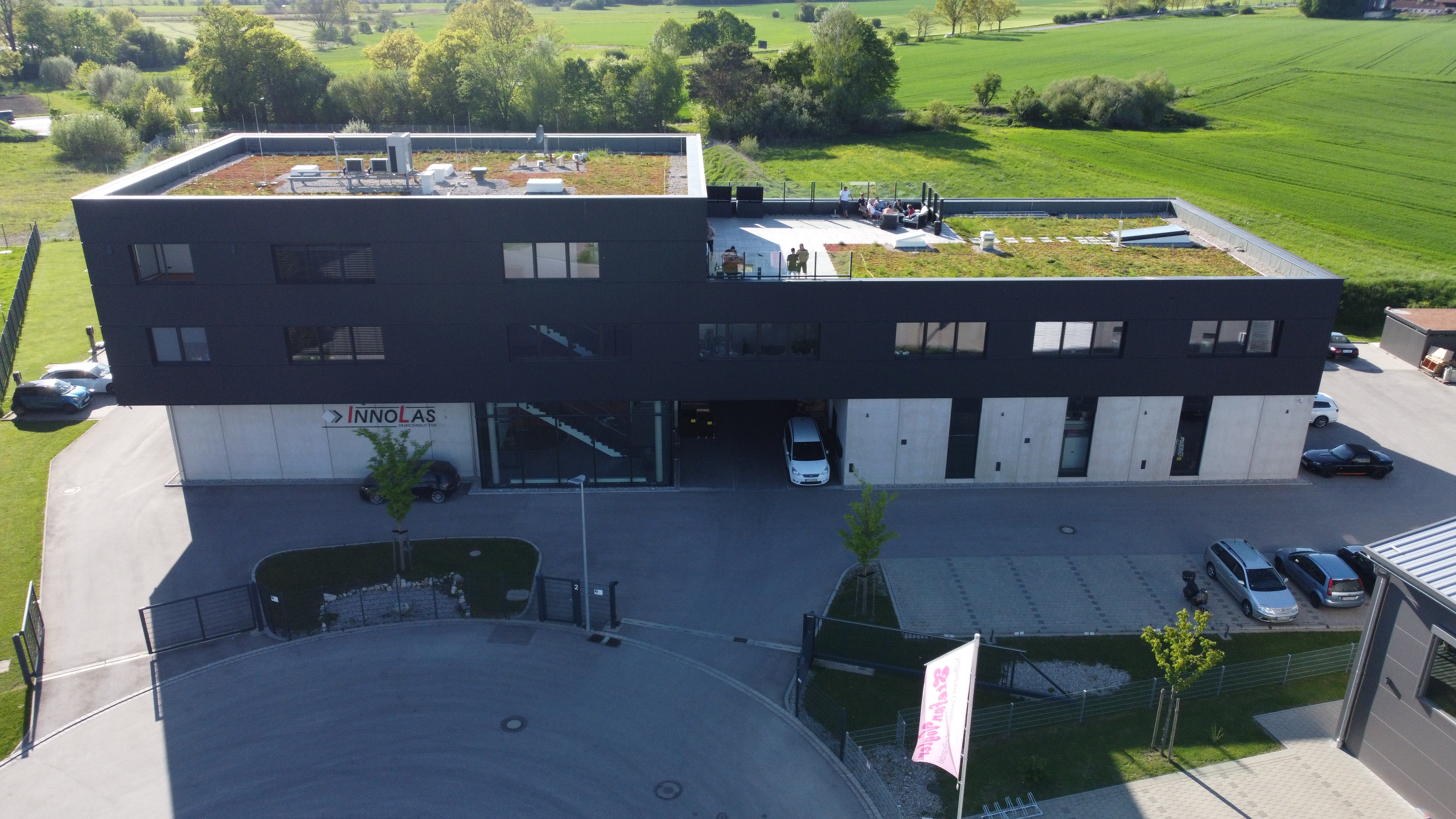
Manufacturer of laser wafer marking and sorting systems for the semiconductor and photovoltaic industries

InnoLas Semiconductor GmbH
Inning am Ammersee (DE) · Karlovac (HR)New on Amplifa
About InnoLas Semiconductor
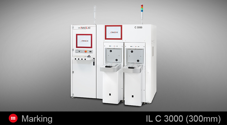
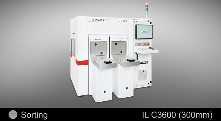
InnoLas Semiconductor GmbH, headquartered in Inning am Ammersee, develops and manufactures wafer marking and wafer sorting systems for the semiconductor and photovoltaic industries. The portfolio covers wafer marking, wafer sorting and wafer inspection: laser systems mark wafers permanently and reliably in-process, sorting systems perform automated classification and handling, and inspection solutions verify wafer quality. The IL-series systems are developed and built in-house and delivered to customers worldwide. In 2023, the company opened a branch in Karlovac, Croatia, to expand its global presence. Operating as a GmbH, InnoLas Semiconductor is internationally active at trade fairs such as SEMICON and serves customers from semiconductor manufacturing and solar module production.
- Site
- Inning am Ammersee
- Processes
- Wafer marking (laser wafer marking), Wafer sorting (wafer sorting systems), Wafer inspection (wafer inspection), Wafer Marking, Wafer Sorting, Wafer Inspection
- Materials
- Laser wafer marking, Wafer sorting systems, Wafer inspection
- Industries
- Semiconductor industry, Photovoltaics
- 01
Engineering & system development
- 02
Manufacturing of marking and sorting systems
- 03
Assembly & integration
- 04
Wafer marking / sorting / inspection as application
- 05
Sales & worldwide support
Technologies & Processes
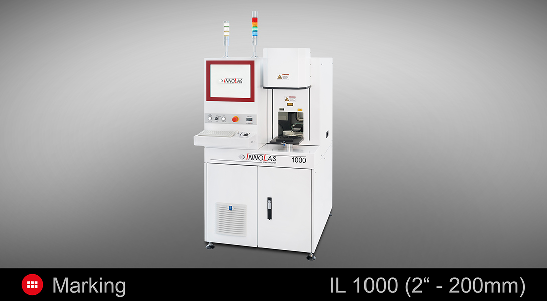
Laser wafer marking
Durable engraving of wafers for traceability in semiconductor manufacturing.
Wafer sorting systems
Automated sorting and handling of wafer batches.
Wafer inspection
Optical inspection of wafer quality during the production process.
Locations
Inning am Ammersee
DEHeadquarters, development & manufacturing
- Materials
- Wafers (semiconductor, photovoltaics)
- Wafer marking systems (IL series)
- Wafer sorting systems
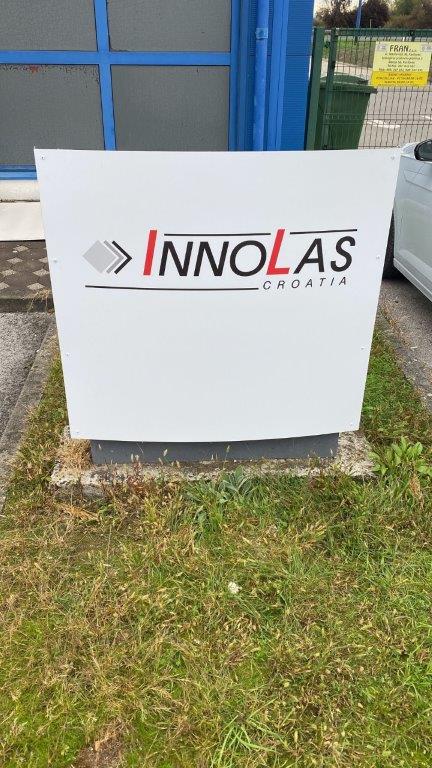
Karlovac
HRBranch office (since 2023)
Systems & Applications
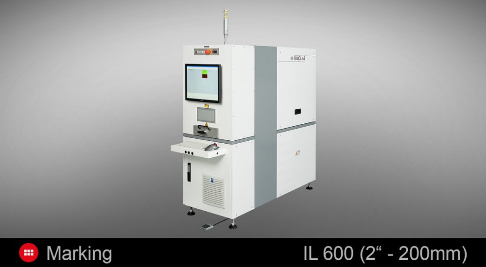
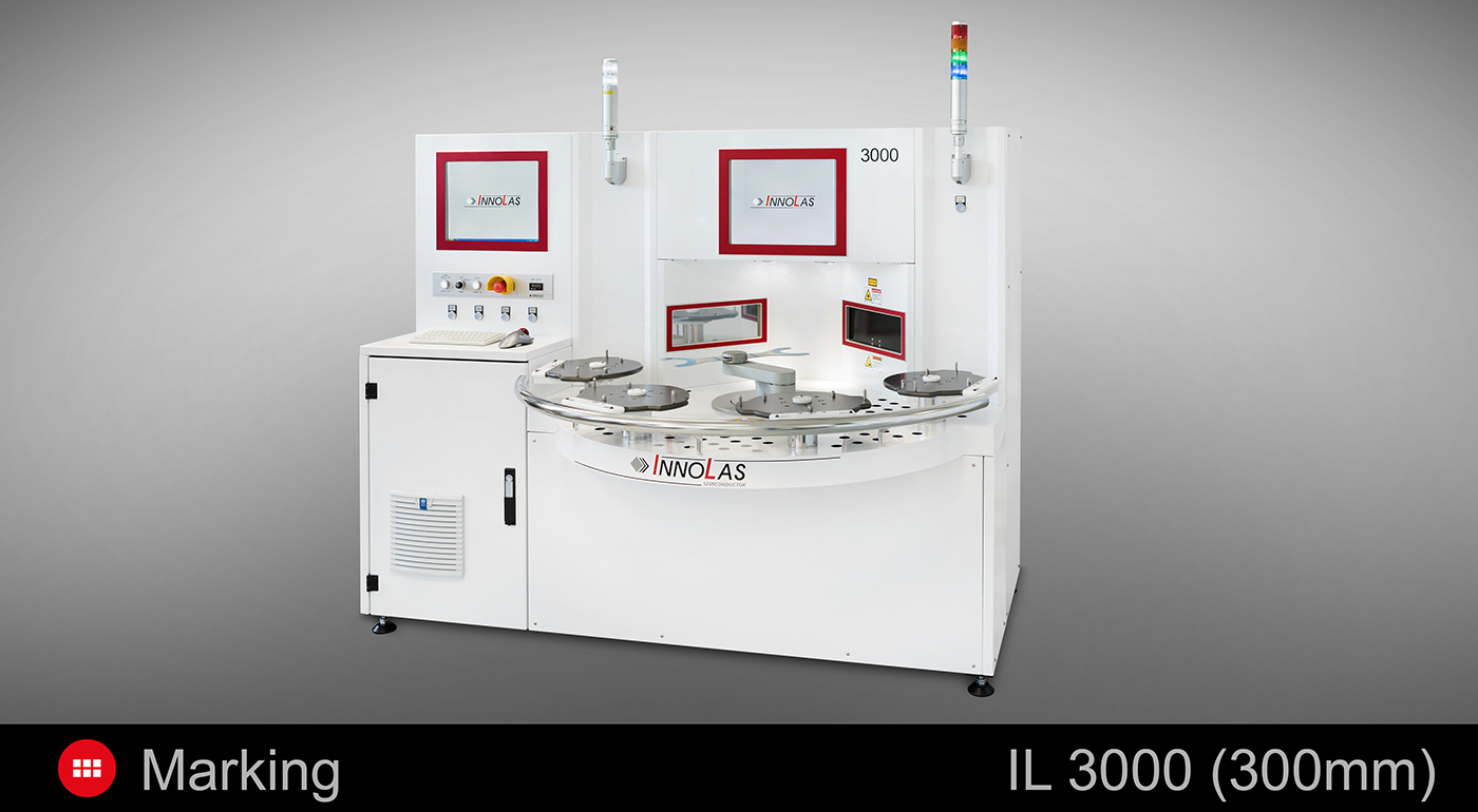
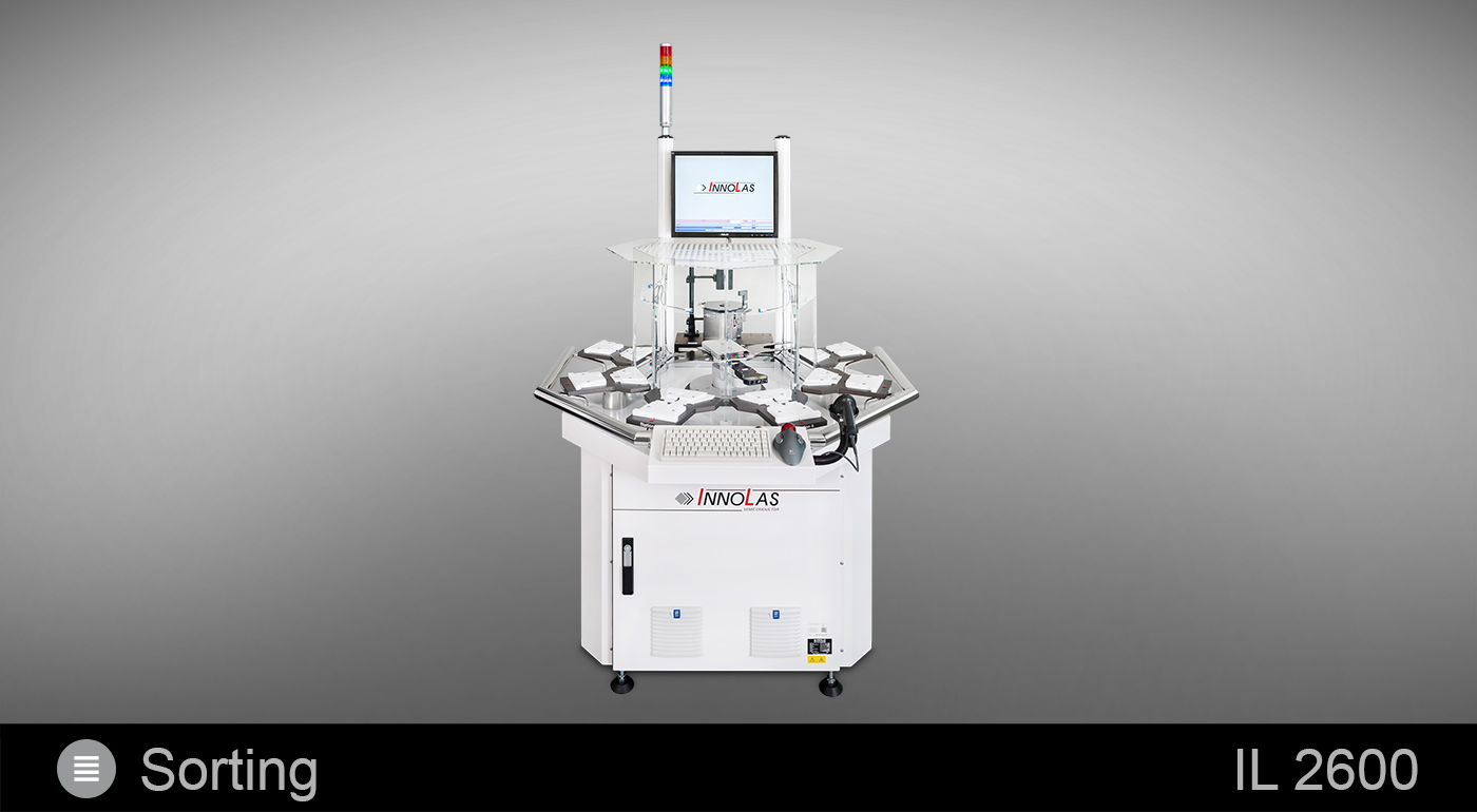
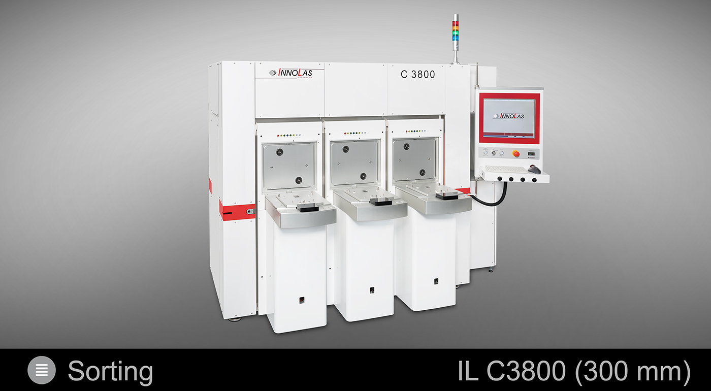
Inside the production
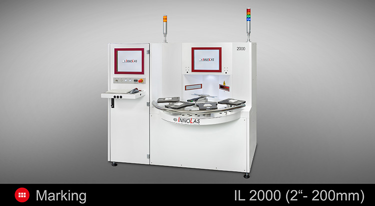
Industries
Processes & technical limits
| Processes | Tolerance | Max. part | Weight | Lot size | Materials |
|---|---|---|---|---|---|
| Wafer marking (laser wafer marking)Surface | – | – | – | – | – |
| Wafer sorting (wafer sorting systems)Assembly | – | – | – | – | – |
| Wafer inspection (wafer inspection)Testing | – | – | – | – | – |
2 Anlagen & Maschinen
| Machine | Manufacturer / model | Quantity | Working area | Year built | Site |
|---|---|---|---|---|---|
| Wafer marking system | InnoLas Semiconductor | – | – | – | Inning am Ammersee |
| Wafer sorting system | InnoLas Semiconductor | – | – | – | Inning am Ammersee |
Additional services
History
- 2023
Opening of the new branch office in Karlovac, Croatia
- 2025
Trade fair participations, among others at SEMICON