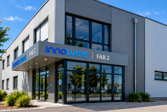
Manufacturer of GaAs-based quantum dot laser diodes and photonic devices from 780 to 1350 nm

Innolume GmbH
Dortmund · San DiegoNew on Amplifa
About Innolume
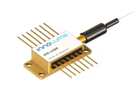
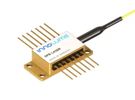
Innolume GmbH is a manufacturer of GaAs-based semiconductor laser diodes and photonic devices with wavelengths from 780 nm to 1350 nm. The portfolio includes single-mode and multimode laser diodes, DFB and FBG lasers, semiconductor and booster optical amplifiers (SOA/BOA), comb lasers, gain chips, superluminescent diodes (SLD), laser diode drivers and pulsed laser turnkey systems. Manufacturing is vertically integrated: from epitaxy with two production-scale MBE reactors, through wafer processing including electron beam lithography and facet coating, to chip packaging as chip-on-carrier or fiber-pigtailed modules — everything is done at the Dortmund facility. The core of the technology is InAs quantum dots in GaAs with AlGaAs barriers, enabling improved properties such as low relative intensity noise and temperature-independent behavior. Innolume develops custom photonic devices, manufactures mid-volume quantities in-house and transfers high-volume production to contract manufacturers. The devices are used in medical diagnostics and therapy, scientific research, industrial manufacturing, cloud network infrastructure and AI systems. The company supplies more than 100 customers worldwide.
- Site
- Dortmund
- Processes
- Epitaxy (MBE, In,Al,Ga,AsP/GaAs heterostructures, InAs quantum dots on GaAs substrates, MOCVD, Wafer front-end processing including electron beam lithography (laser chips), Facet coating (surface passivation of cleaved facets, anti-reflection coating <0.01% reflectivity,, Chip packaging: chip-on-carrier (CoC) and fiber-pigtailed modules, burn-in and quality control, Device characterization/testing: LIV curves, far/near field, PER, optical spectra, noise figure,, Design and development of custom photonic devices (custom design,, Custom design of tailored photonic devices, Mid-volume manufacturing in-house, transfer to contract manufacturing for high volume
- Materials
- GaAs (gallium arsenide), InGaAs (indium gallium arsenide), InAs (indium arsenide, quantum dots), AlGaAs (aluminium gallium arsenide, barriers), In,Al,Ga,AsP/GaAs heterostructures, Gallium arsenide, Indium arsenide, Indium gallium arsenide
- Certificates
- Burn-in & outgoing QC
- Founded
- 2003
- Industries
- Medical technology (diagnostics and therapy), Scientific research, Industrial manufacturing, Data communications / cloud network infrastructure, Artificial intelligence
- 01
Custom Design & Device Modelling
- 02
Epitaxy (MBE)
- 03
Wafer front-end processing
- 04
Facet coating / passivation
- 05
Chip packaging (CoC, fiber-pigtailed modules)
- 06
Burn-in & quality control
- 07
Device characterization
Material Systems & Processes
Gallium arsenide
Substrate material for all laser chips and heterostructures.
Indium arsenide
Forms the self-organized quantum dots as the active gain medium.
Indium gallium arsenide
Quantum well structures for the wavelength range 780–1120 nm.
Aluminium gallium arsenide
Barrier layers around the quantum dots in the heterostructures.
Molecular beam epitaxy
Epitaxy of In,Al,Ga,AsP/GaAs heterostructures on two production-scale reactors.
Electron beam lithography
Front-end wafer processing for high-quality laser chips.
Locations
Dortmund
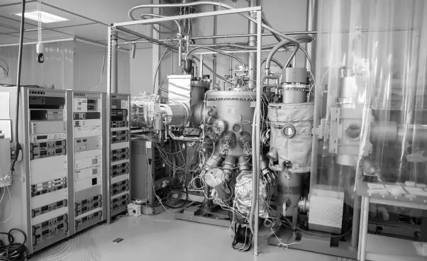
DEHeadquarters, semiconductor laser fab (epitaxy, wafer processing, packaging)
- Lot size
- Small to mid-volume series in-house; high volume via contract manufacturing
- Materials
- InAs/GaAs, InGaAs, AlGaAs
- 2 production-scale MBE epitaxy reactors
- Electron beam lithography
- Facet coating/passivation
- Chip packaging
- Measurement and characterization equipment
San Diego
USSales representative office (Axalume Inc.)
Components
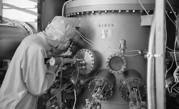
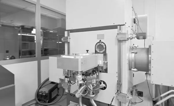
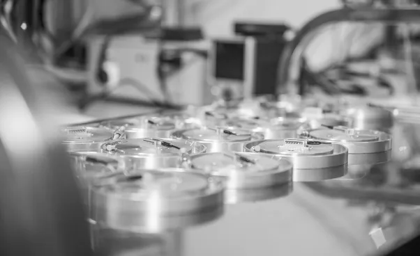
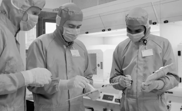
Inside the production
Industries
Processes & technical limits
| Processes | Tolerance | Max. part | Weight | Lot size | Materials |
|---|---|---|---|---|---|
| Epitaxy (MBE, In,Al,Ga,AsP/GaAs heterostructures, InAs quantum dots on GaAs substrates, MOCVDEngineering | – | – | – | – | GaAs, InAs, InGaAs, AlGaAs, In,Al,Ga,AsP/GaAs |
| Wafer front-end processing including electron beam lithography (laser chips)Engineering | – | – | – | – | GaAs, InGaAs/GaAs |
| Facet coating (surface passivation of cleaved facets, anti-reflection coating <0.01% reflectivity,Surface | – | – | – | – | GaAs, InGaAs/GaAs |
| Chip packaging: chip-on-carrier (CoC) and fiber-pigtailed modules, burn-in and quality controlAssembly | – | – | – | Low volumes – mid-volume, via Contract Manufacturing | GaAs, InGaAs/GaAs |
| Device characterization/testing: LIV curves, far/near field, PER, optical spectra, noise figure,Testing | – | – | – | – | – |
| Design and development of custom photonic devices (custom design,Engineering | – | – | – | – | – |
1 Anlagen & Maschinen
| Machine | Manufacturer / model | Quantity | Working area | Year built | Site |
|---|---|---|---|---|---|
| MBE epitaxy reactor (Production-scale MBE reactor) | – | 2 | – | – | Dortmund, Konrad-Adenauer-Allee 11 |
Additional services
Quality
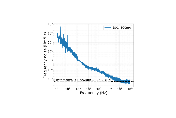
Every module undergoes a burn-in procedure and outgoing quality control before shipping. Device characterization includes, among other things, LIV curves, far/near field, PER, optical spectra, noise figure, RIN as well as frequency and phase noise.
| Evidence | Dortmund |
|---|---|
| Burn-in & outgoing QC |
History
- 2003
Foundation; Innolume was the first team to bring quantum dot semiconductor devices to market commercially