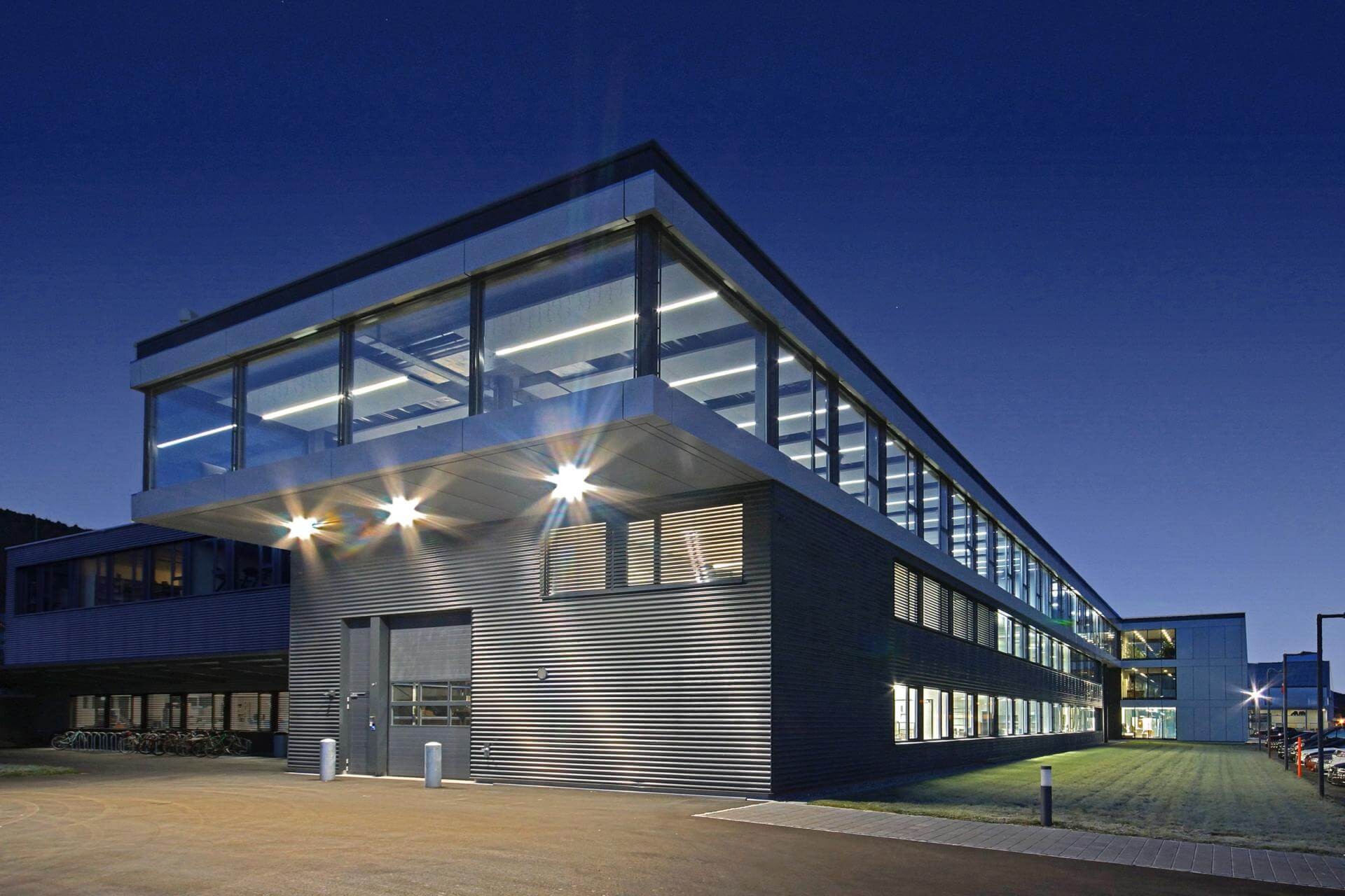
Development and manufacture of physical, chemical and biological sensors in thin-film, thick-film and MEMS technology.
Innovative Sensor Technology IST AG
Ebnat-Kappel (CH) · Roznov pod Radhostem (CZ) · Las Vegas (US) · Shanghai (CN) · Freiburg (DE) · Berlin (DE) · Dresden (DE) · Fehraltorf (CH)New on Amplifa
About Innovative Sensor Technology IST AG
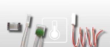
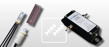
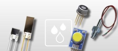
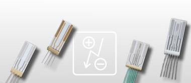
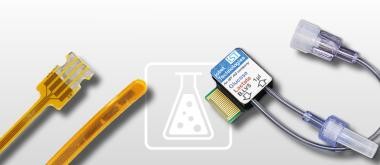
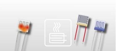
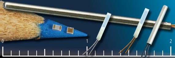
Innovative Sensor Technology IST AG is a manufacturer of physical, chemical and biological sensors founded in 1991 and headquartered in Ebnat-Kappel, Switzerland. The company develops and manufactures temperature sensors (thin- and thick-film RTDs made of platinum and nickel), thermal mass flow sensors, capacitive humidity sensors and modules, conductivity sensors and biosensors, as well as microheaters and thermal infrared emitters. Production takes place in cleanrooms (ISO 5, over 1,000 m²) using sputter/PVD coating, photolithography, etching technology, laser trimming, screen printing, wafer bonding and MEMS processes on ceramic and silicon substrates. In addition to standard products, iST offers custom sensor developments, signal processing, assembly, factory calibration and 100% end-of-line product inspection. Since 2005, the company has belonged to the Endress+Hauser Group and employs around 500 people worldwide at locations in Switzerland, the Czech Republic, the USA, China and Germany.
- Site
- Ebnat-Kappel
- Processes
- Thin- and thick-film technology (manufacture of physical, chemical and biological sensors), Thick-film technology (screen printing) for sensors, microheaters, circuit boards, Thin-film technology (PVD & CVD, sputtering, electroplating, sol-gel), Photolithography, Etching (ion etching, wet chemical etching), Laser trimming / laser calibration, Screen printing (contact points, passivation), Cutting (dicing of the substrates)
- Materials
- Platinum, Nickel, Silicon, Polysilicon, SiN (silicon nitride), Aluminum, AlN (aluminum nitride, piezoelectric), Ceramic (substrates, ceramic PCBs)
- Certificates
- ISO 9001:2015, ISO 14001:2015, ISO 13485:2016, ESCC qualification (Hi-Rel space sensors), ISO 9001, ISO 14001, ISO 13485, EN 9100, Other (ESCC qualification Hi-Rel space sensors)
- Founded
- 1991
- Employees
- 500
- Industries
- Medical technology, Process control/process engineering, Automation technology, Electric vehicles (EVs), Aerospace, Test and measurement technology
- 01
Consulting & feasibility assessment
- 02
Custom sensor design
- 03
Substrate coating (sputtering/PVD & CVD)
- 04
Photolithography
- 05
Etching (ion etching, wet chemical)
- 06
Laser trimming / laser calibration
- 07
Screen printing (contacts, passivation)
- 08
Cutting of the substrates
- 09
Wire bonding / welding
- 10
Assembly (probes, flow cells, housings)
- 11
Factory calibration & 100% end-of-line product inspection
- 12
Delivery & after-sales support
Materials & Processes
Platinum
Active sensor material for thin- and thick-film RTDs and heaters on ceramic and silicon substrates.
Nickel
Material for nickel temperature sensors, with which the company entered the sensor market in 1991.
Silicon
Substrate material for MEMS sensors, including 150 mm wafers for Pt/Ni sensor structures.
Silicon nitride
Membrane material for thermopiles and thermal flow sensors.
Aluminum nitride (piezoelectric)
Piezoelectric material for resonant MEMS gas sensor chips.
Aluminum
Used in polysilicon-aluminum thermopiles for flow detection.
Ceramic (substrates, ceramic PCBs)
Carrier material for thin- and thick-film sensors as well as packaging circuit boards.
Stainless steel
Housing material for pressure-tight humidity modules such as the HYT 939.
Polymer
Sensor material of capacitive humidity sensors.
Locations
Ebnat-Kappel
CHHeadquarters: R&D, production, sales, administration
- Lot size
- Small series of custom sensors through to mass production
- Materials
- Platinum, nickel, silicon, ceramic
- Sputter/PVD deposition systems (150 mm silicon substrates)
- Fully automatic thick-film production lines
- Cleanroom ISO 5 (>1,000 m²), production area 3,700 m²
- SEM/EDX, XRF, µCT, 3D laser microscopy
Roznov pod Radhostem
CZProduction site (assembly)
Las Vegas
USSales office and Application Support Center
Shanghai
CNSales office and Application Support Center
Freiburg
DESubsidiary iST Jobst (microsystems technology/electrochemical analytics)
Berlin
DESubsidiary iST Innuscreen (nucleic acid extraction, molecular diagnostics)
Dresden
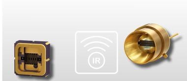
DESubsidiary Infrasolid GmbH (thermal infrared emitters)
Fehraltorf
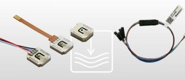
CHSubsidiary Senstech AG (force, pressure, strain and displacement sensors)
Sensor Products

Inside the production


Industries
Processes & technical limits
| Processes | Tolerance | Max. part | Weight | Lot size | Materials |
|---|---|---|---|---|---|
| Thin- and thick-film technology (manufacture of physical, chemical and biological sensors)Engineering | – | – | – | Mass production | Platinum, Nickel, Ceramic, Silicon |
| Thick-film technology (screen printing) for sensors, microheaters, circuit boardsEngineering | – | – | – | High volumes (mass production) | Ceramic substrates, PTC materials, conductive pastes |
| Thin-film technology (PVD & CVD, sputtering, electroplating, sol-gel)Surface | – | – | – | – | Platinum, Nickel, Ceramic substrates |
| PhotolithographyEngineering | – | – | – | – | Photoresist |
| Etching (ion etching, wet chemical etching)Surface | – | – | – | – | – |
| Laser trimming / laser calibrationEngineering | – | – | – | – | – |
| Screen printing (contact points, passivation)Engineering | – | – | – | – | conductive paste, non-conductive paste |
| Cutting (dicing of the substrates)Engineering | – | – | – | – | – |
| Welding (wire bonding to sensors)Joining | – | – | – | – | bare wires, insulated wires |
| Measurement and calibration (2-point calibration measurement, resistance testing)Testing | – | – | – | 100% end-of-line product inspection | – |
| PVDSurface | – | – | – | – | Platinum, Nickel |
| CVD / LPCVD / PECVDSurface | – | – | – | – | – |
| Thermal oxidationSurface | – | – | – | – | Silicon |
| LithographyEngineering | – | – | – | – | – |
| Dry etching (RIE, DRIE)Surface | – | – | – | – | Silicon |
| Wafer bonding and wafer dicingJoining | – | – | – | – | Silicon |
| MEMS integration / packaging (ceramic PCBs, soldering, brazing, wire bonding)Assembly | – | – | – | – | Ceramic, Silicon, AlN, Aluminum |
| Manufacture of silicon-based MEMS sensors (thermopiles, piezoresistive strain gauges,Engineering | – | – | – | several thousand sensors/year – several million sensors/year | Silicon, Polysilicon, SiN, Aluminum, Platinum, AlN |
| Development and manufacture of temperature sensors (thin/thick-film RTDs made of platinum andEngineering | – | – | – | – | Platinum, Nickel |
| Manufacture of humidity sensors and modules (capacitive)Engineering | – | – | – | – | Polymer |
| Manufacture of thermal mass flow sensorsEngineering | – | – | – | – | Polysilicon, SiN |
| Manufacture of conductivity sensors and biosensorsEngineering | – | – | – | – | – |
| Manufacture of microheaters (thick film)Engineering | – | – | – | – | – |
| Manufacture of thermal infrared emitters (Infrasolid)Engineering | – | – | – | – | – |
| Component overmolding in electronics (plastic overmolding of sensors)Plastics | – | – | – | – | – |
| Application-specific factory calibrationTesting | – | – | – | – | – |
5 Anlagen & Maschinen
| Machine | Manufacturer / model | Quantity | Working area | Year built | Site |
|---|---|---|---|---|---|
| Sputter/deposition system (PVD) | – | – | 150 mm silicon substrates (platinum/nickel coating) | – | Ebnat-Kappel, Switzerland |
| Fully automatic thick-film production lines | – | – | – | – | Ebnat-Kappel, Switzerland |
| Cleanroom ISO 5 (>1'000 m²) with production area of 3'700 m² | – | – | 13'500 m² development and production area | – | Ebnat-Kappel, Switzerland |
| Analysis tools (SEM/EDX, XRF, µCT, 3D laser microscopy) | – | – | – | – | Ebnat-Kappel, Switzerland |
| Production facility (assembly) | – | – | – | 1994 | Roznov pod Radhoštěm, Czech Republic |
Additional services
Reference customers
Quality & Certifications
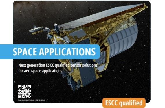
iST is certified to ISO 9001:2015 (quality) and ISO 14001:2015 (environment); in addition, it holds the ISO 13485:2016 certification as well as ESCC qualification for Hi-Rel space sensors. Process and product inspections take place at all stages of manufacturing, including 100% end-of-line product inspection with 2-point calibration; analysis tools such as SEM/EDX, XRF, µCT and 3D laser microscopy are available in-house.
| Evidence | Ebnat-Kappel |
|---|---|
| ISO 9001 | |
| ISO 14001 | |
| ISO 13485 | |
| EN 9100 | |
| Other (ESCC qualification Hi-Rel space sensors) |
History
- 1991
Founding of Innovative Sensor Technology IST AG in Wattwil, Switzerland; entry into the sensor market with nickel temperature sensors
- 1993
Start of development and production of platinum temperature sensors
- 1994
Opening of the production facility (assembly) in Roznov pod Radhoštěm, Czech Republic; start of flow sensor development
- 1995
Sales launch in Las Vegas, USA through an exclusive representative
- 1999
Start of development and production of humidity sensors
- 2004
Start of development and production of conductivity sensors and humidity modules
- 2005
Acquisition of iST by the Endress+Hauser Group
- 2006
Founding of a 100-percent-owned subsidiary in Las Vegas, USA
- 2012
Relocation of headquarters from Wattwil to the company's own new building in Ebnat-Kappel
- 2015
Acquisition of Jobst Technologies GmbH in Freiburg, Germany; opening of sales offices in Shanghai (China) and Prague (Czech Republic)
- 2019
iST moves into the expanded headquarters
- 2020
Acquisition of AJ Innuscreen in Berlin, Germany; renamed IST Innuscreen GmbH
- 2022
Infrasolid GmbH in Dresden and Senstech AG in Fehraltorf become part of the iST Group
- 2024
Introduction of the new branding