Optical systems, micro-optics, lasers and optoelectronic modules for semiconductors, medical technology, metrology and smart mobility
JENOPTIK AG
Jena · Berlin · Dresden · Triptis · Augsburg · Monheim am Rhein · Villingen-Schwenningen · Wedel · Wetzlar · AlgiersNew on Amplifa
About Jenoptik
JENOPTIK AG is a publicly listed technology group headquartered in Jena, active in the photonics market. The company develops and manufactures optical systems and micro-optics, optical thin-film elements, diffractive optical elements and high-power lasers – from epitaxial wafer production and the manufacture of optical components through to cleanroom assembly of complete systems. Processes include precision optics made from optical glasses, crystals and plastics, coating and filter production from DUV to FIR, injection molding of polymer optics, laser material processing, toolmaking and optomechatronic assembly. Customers include OEMs from semiconductor equipment, medical technology and life science, automotive, mechanical engineering, metrology, aerospace as well as security and defense technology; in the field of traffic enforcement, the group also offers measurement systems, calibration and services. As an OEM development and production partner, Jenoptik covers the entire value chain including supply chain management for its customers. In Germany, the group manufactures at sites in Jena, Berlin, Dresden, Triptis, Augsburg, Monheim am Rhein, Villingen-Schwenningen, Wedel and Wetzlar; worldwide locations exist in Europe, America, Africa and Asia-Pacific.
- Site
- Jena
- Processes
- Laser systems for cutting of plastics, metals and sensitive materials, Laser welding of plastics, metals and sensitive materials, Laser perforating of plastics, metals and sensitive materials, Laser marking, Laser welding (of metal and plastic), Laser cutting, Laser drilling, Laser structuring and removal
- Materials
- Optical glass SiO2, Silicon, Germanium, Zinc selenide, Sapphire, Magnesium fluoride, Calcium fluoride, GaAs compound semiconductors (Al, In, Ga)(As, P)
- Certificates
- ISO 9001:2015, ISO 14001:2015, ISO 50001:2018, ISO 13485:2016, ISO 9001:2015 (JENOPTIK Optical Systems LLC, Huntsville, USA), ISO 9001:2015 (JENOPTIK Optical Systems LLC, Jupiter, USA), ISO 9001:2015 (JENOPTIK Shanghai), ISO 37301 (compliance management), AEO-F (Authorized Economic Operator, JENOPTIK Robot GmbH), TISAX (information security automotive), ISO 9001, ISO 14001, ISO 13485, ISO 50001, TISAX, ISO 45001
- Founded
- 1990 (JENO
- Employees
- 4,500 (worldwide,
- Industries
- Semiconductor and semiconductor equipment, Medical technology and life science, Automotive and suppliers, Mechanical and plant engineering, Industrial metrology, Traffic safety and smart mobility
- 01
Engineering and OEM co-development
- 02
Epitaxial wafer growth and semiconductor manufacturing
- 03
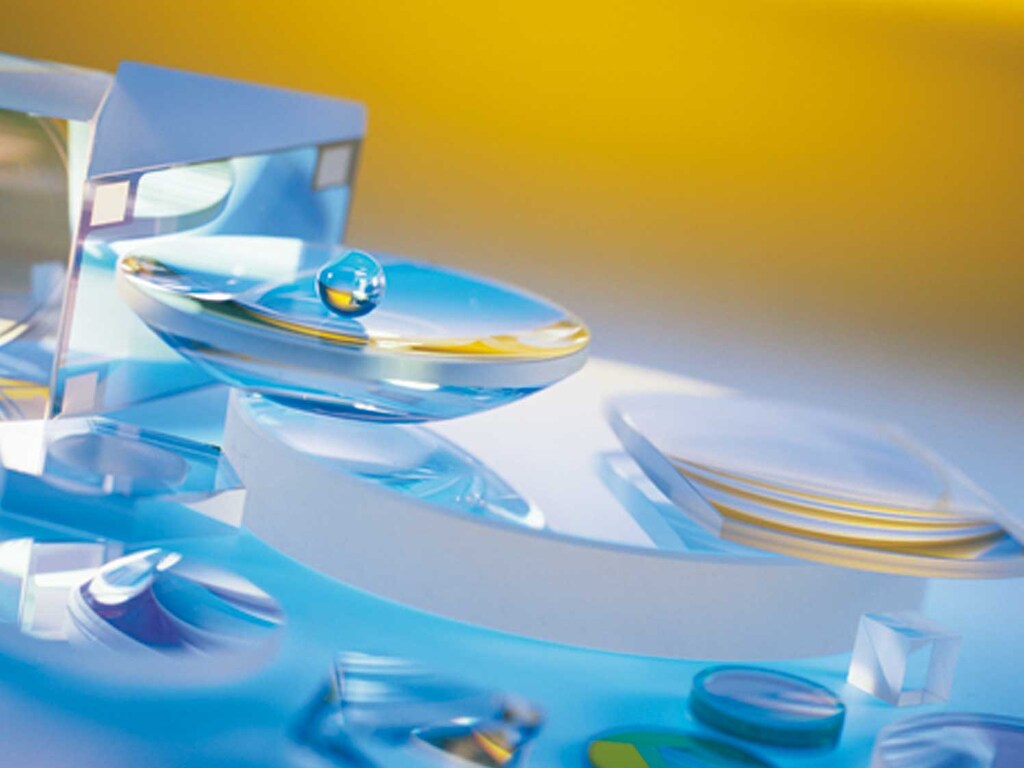
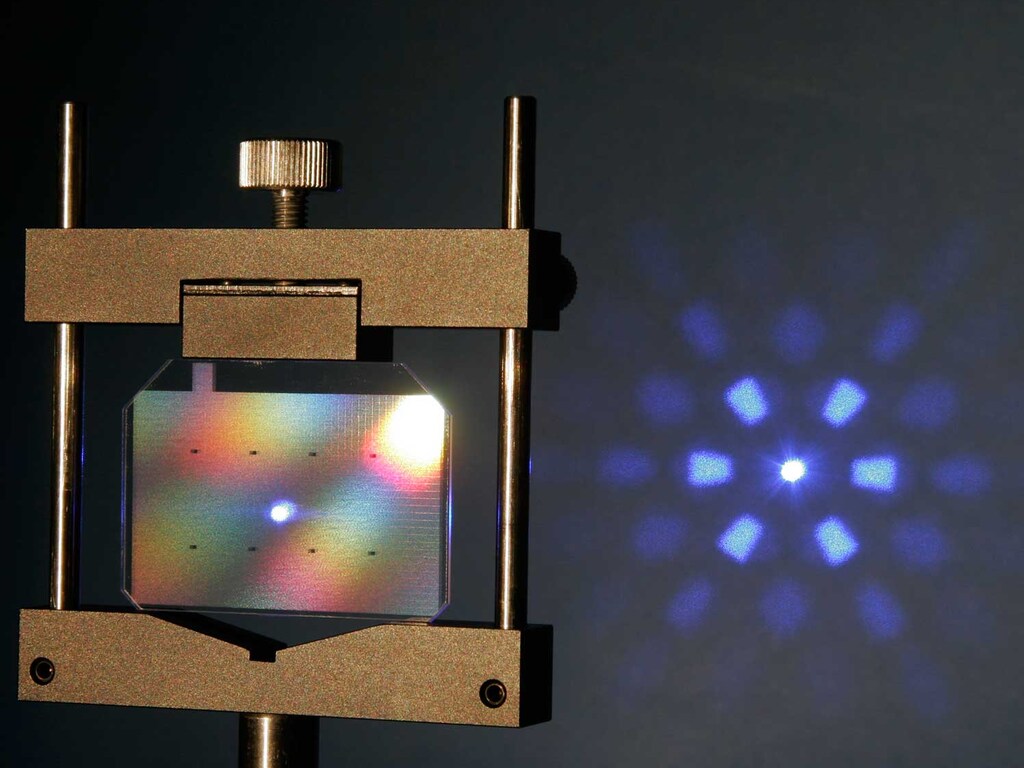
Optics and micro-optics manufacturing
- 04
Optical coating and filter production
- 05
Injection molding of polymer optics and toolmaking
- 06
Laser material processing
- 07
Assembly and integration (cleanroom)
- 08
Inspection, test and calibration technology
- 09
Supply chain management and customer service
Materials and Processes
Optical glass (SiO2)
Base material for precision optical components and systems.
Silicon
Optical material for infrared and semiconductor applications.
Germanium
Infrared-optical material for thermal applications.
Zinc selenide
IR-transparent material for laser and thermal optics.
Magnesium fluoride
Crystalline material for optical components from UV to IR.
Calcium fluoride
Crystalline material for high-resolution UV optics.
GaAs compound semiconductors (Al, In, Ga)(As, P)
Substrate material for laser bars and single emitters.
Nd:YVO4
Laser crystal for frequency-doubled thin-disk lasers.
Optical plastics (polymers)
Injection-molded polymer optics for miniaturized systems.
Diamond-Like Carbon (DLC)
Wear-resistant coating for optical surfaces.
Components
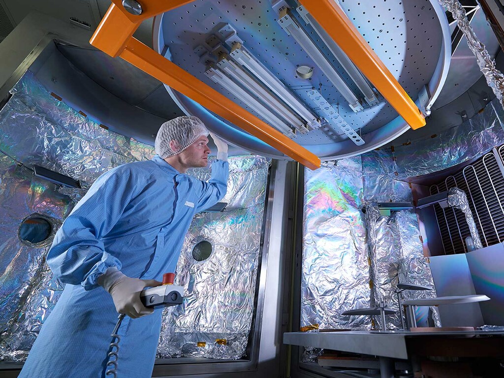
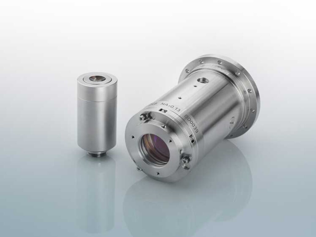
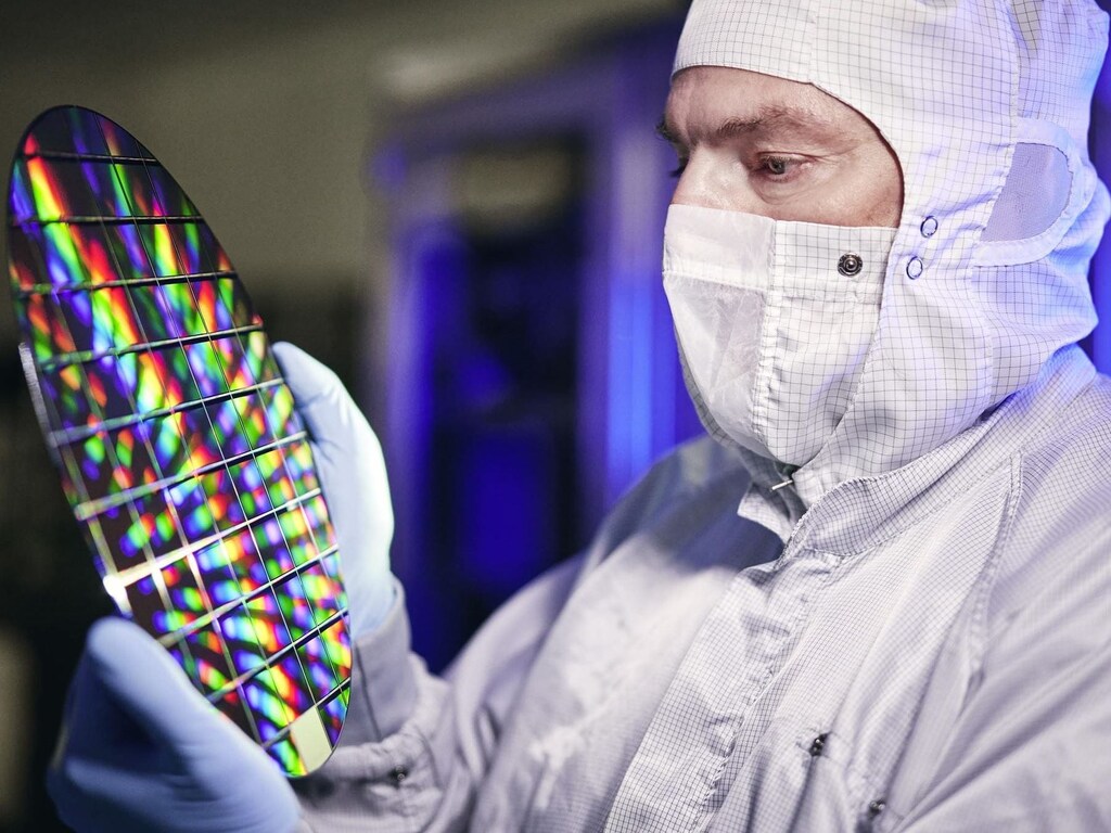
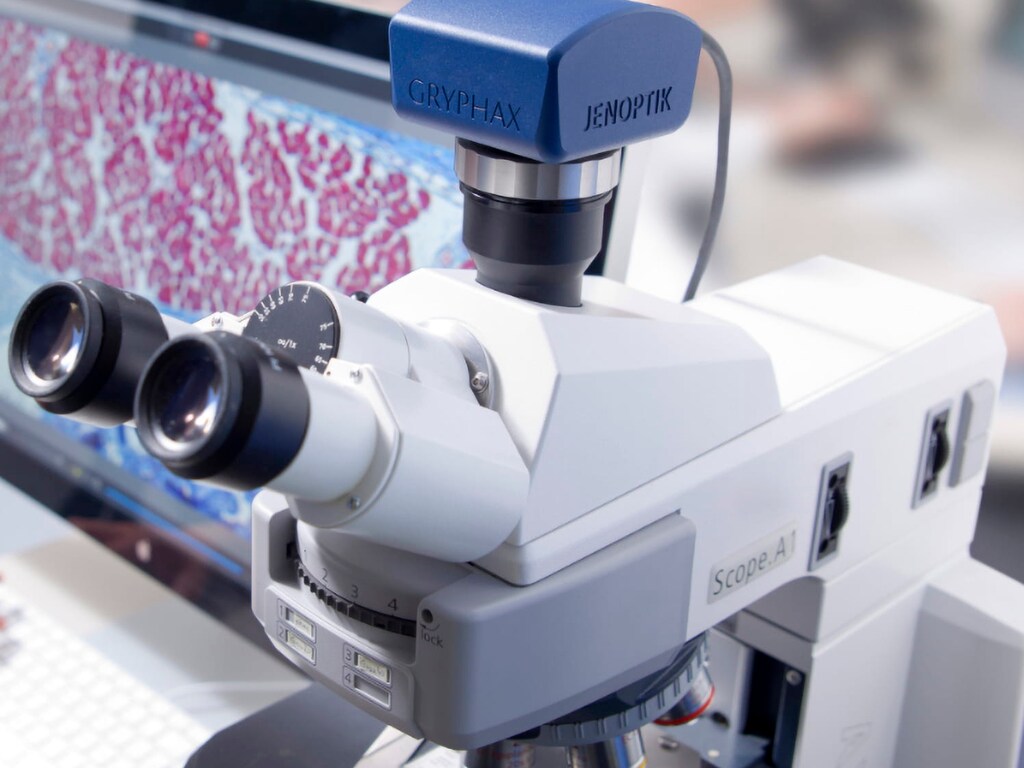
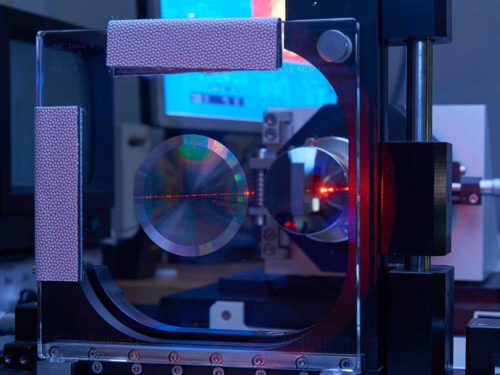
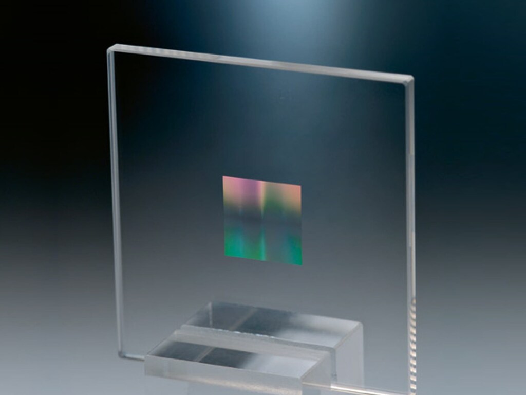
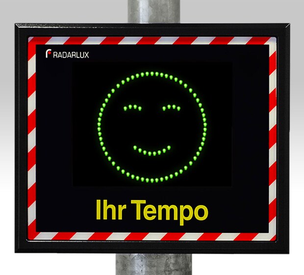
Inside the production
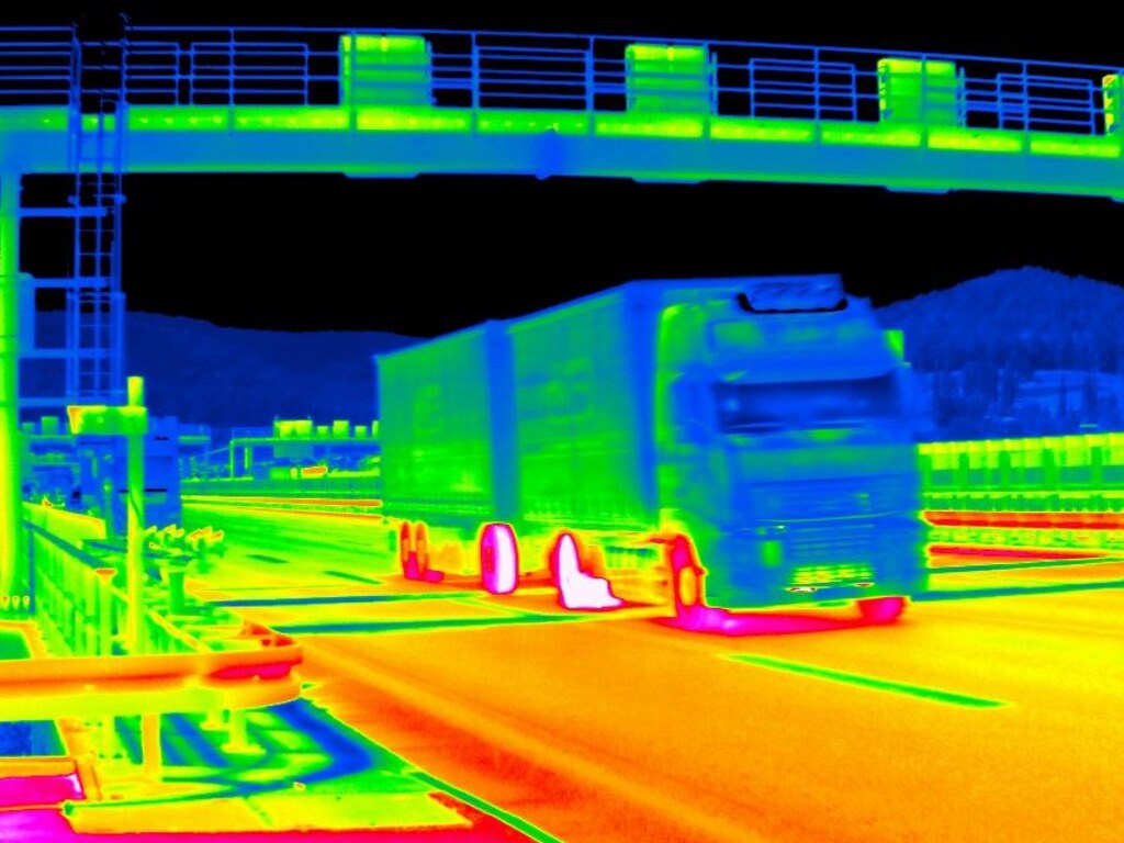
Industries
Processes & technical limits
| Processes | Tolerance | Max. part | Weight | Lot size | Materials |
|---|---|---|---|---|---|
| Laser systems for cutting of plastics, metals and sensitive materialsLaser material processing | – | – | – | – | plastics, metals, sensitive materials |
| Laser welding of plastics, metals and sensitive materialsLaser material processing | – | – | – | – | plastics, metals, sensitive materials |
| Laser perforating of plastics, metals and sensitive materialsLaser material processing | – | – | – | – | plastics, metals, sensitive materials |
| Laser markingLaser material processing | – | – | – | – | metals, polymers, substrates, ceramics |
| Laser welding (of metal and plastic)Laser material processing | – | – | – | – | metal, plastic |
| Laser cuttingLaser material processing | – | – | – | – | plastic, metal |
| Laser drillingLaser material processing | – | – | – | – | metals, polymers, substrates, ceramics |
| Laser structuring and removalLaser material processing | – | – | – | – | metals, polymers, substrates, ceramics |
| Selective laser solderingJoining | – | – | – | – | – |
| Laser engravingLaser material processing | – | – | – | – | – |
| Laser cleaningLaser material processing | – | – | – | – | – |
| Laser ablationLaser material processing | – | – | – | – | – |
| Laser scoring for airbag applications (contact-free processing of plastic components)Laser material processing | – | – | – | – | plastic |
| Laser tire carvingLaser material processing | – | – | – | – | rubber/tires |
| Epitaxial wafer growth (compound semiconductors (Al, In, Ga)(As, P))Semiconductor manufacturing | – | – | – | – | GaAs, AlGaAs, InGaAsP |
| Semiconductor fab for processing GaAs-based optoelectronic devices; manufacture of compoundSemiconductor manufacturing | – | – | – | – | GaAs |
| High-power diode laser assembly and packaging (760-1060 nm, output power levels up to 300 W in cwLaser manufacturing | – | – | – | – | GaAs, AlGaAs |
| Manufacture of diode-pumped thin disk lasers (frequency-doubled 532 nm thin disk Nd:YVO4 lasers)Laser manufacturing | – | – | – | – | Nd:YVO4 |
| Manufacture of fiber lasers (JenLas fiber ns 25-105 for industrial marking and micromachining)Laser manufacturing | – | – | – | – | – |
| Manufacturing of optical coatings and filters (narrowband and bandpass filters, edge filters,Coating | – | – | – | – | optical glass, polymer optics |
| Diamond-like carbon (DLC) coating of opticsCoating | – | – | – | – | optical glass |
| Injection molding of sophisticated polymer optical componentsInjection molding | – | – | – | – | plastic/polymers |
| Development and production of high-precision injection molding (endoscopy miniaturization)Injection molding | accuracy of 1 µm for chip-prism assembly | – | – | – | plastic/polymers |
| Tool and mold design and constructionToolmaking | – | – | – | – | – |
| Surface technologySurface treatment | – | – | – | – | – |
| Opto-mechanical and optoelectronic assembly; cleanroom assemblyAssembly | – | – | – | – | – |
| Manufacture of optical systems, micro-optics and high-end objective lenses (DUV to FIR); opticalOptics manufacturing | – | – | – | – | optical glass (SiO2, Si, Ge, ZnSe, Sapphire, MgF2, CaF2), polymers |
| State-of-the-art alignment and bonding technologies (chip-prism assembly for endoscopy,Assembly | accuracy of 1 µm for the entire chip-prism assembly | – | – | – | – |
| Assembly of laser system components (from laser components to automated laser machines, robot-basedAssembly | – | – | – | – | – |
| Development, manufacturing and sales of optical test & measurement instruments and equipment forMeasuring and testing technology | – | – | – | – | – |
| Development, production, sales and service of industrial metrology productsMeasuring and testing technology | – | – | – | – | – |
| Manufacture of optomechatronic assemblies for medical applicationsAssembly | – | – | – | – | – |
| Manufacture of hardware and software systems and components of optics, laser technology, digitalOptics manufacturing | – | – | – | – | – |
| Manufacture of exhaust air purification systems (removal of pollutants and aerosols from productionSystem manufacturing | – | – | – | – | – |
| Assembly and alignment of LiDAR systems (TRIOPTICS application-oriented solution for alignment andAssembly | – | – | – | – | – |
Additional services
Reference customers
Quality and Certifications
The quality management systems of the business divisions are audited annually; 100% of manufacturing sites are certified to ISO 9001 or ISO 13485. Inspection and calibration technology, including TRIOPTICS measurement equipment and DAkkS-DKD accreditation of industrial metrology, monitors products and processes.
| Evidence | Jena | Berlin | Dresden | Triptis | Villingen-Schwenningen | Wedel | Wetzlar |
|---|---|---|---|---|---|---|---|
| ISO 9001 | |||||||
| ISO 14001 | |||||||
| ISO 13485 | |||||||
| ISO 50001 | |||||||
| TISAX | |||||||
| ISO 45001 |
History
- 1846
Carl Zeiss opens his optical workshop in Jena – the origin of the company.
- 1948
Carl Zeiss Foundation and a new Zeiss company in Baden-Württemberg; the Zeiss plant in Jena becomes public property.
- 1990
Founding of JENOPTIK Carl Zeiss Jena GmbH.
- 1991
Formation of JENOPTIK GmbH as a state-owned enterprise.
- 1996
JENOPTIK AG is established.
- 1998
IPO of JENOPTIK AG on the Frankfurt Stock Exchange.
- 2020
RADARLUX Radar Systems GmbH is merged into JENOPTIK Robot GmbH as of 10.08.2020.